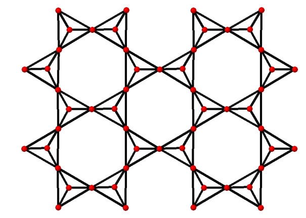
Humanity has always benefited from an intercapillary study in the quantification of natural occurrences in mathematics and other pure scientific fields. Graph theory was extremely helpful to other studies, particularly in the applied sciences. Specifically, in chemistry, graph theory made a significant contribution. For this, a transformation is required to create a graph representing a chemical network or structure, where the vertices of the graph represent the atoms in the chemical compound and the edges represent the bonds between the atoms. The quantity of edges that are incident to a vertex determines its valency (or degree) in a graph. The degree of uncertainty in a system is measured by the entropy of a probability. This idea is heavily grounded in statistical reasoning. It is primarily utilized for graphs that correspond to chemical structures. The development of some novel edge-weighted based entropies that correspond to valency-based topological indices is made possible by this research. Then these compositions are applied to clay mineral tetrahedral sheets. Since they have been in use for so long, corresponding indices are thought to be the most effective methods for quantifying chemical graphs. This article develops multiple edge degree-based entropies that correlate to the indices and determines how to modify them to assess the significance of each type.
Citation: Qingqun Huang, Muhammad Labba, Muhammad Azeem, Muhammad Kamran Jamil, Ricai Luo. Tetrahedral sheets of clay minerals and their edge valency-based entropy measures[J]. Mathematical Biosciences and Engineering, 2023, 20(5): 8068-8084. doi: 10.3934/mbe.2023350
Humanity has always benefited from an intercapillary study in the quantification of natural occurrences in mathematics and other pure scientific fields. Graph theory was extremely helpful to other studies, particularly in the applied sciences. Specifically, in chemistry, graph theory made a significant contribution. For this, a transformation is required to create a graph representing a chemical network or structure, where the vertices of the graph represent the atoms in the chemical compound and the edges represent the bonds between the atoms. The quantity of edges that are incident to a vertex determines its valency (or degree) in a graph. The degree of uncertainty in a system is measured by the entropy of a probability. This idea is heavily grounded in statistical reasoning. It is primarily utilized for graphs that correspond to chemical structures. The development of some novel edge-weighted based entropies that correspond to valency-based topological indices is made possible by this research. Then these compositions are applied to clay mineral tetrahedral sheets. Since they have been in use for so long, corresponding indices are thought to be the most effective methods for quantifying chemical graphs. This article develops multiple edge degree-based entropies that correlate to the indices and determines how to modify them to assess the significance of each type.

| [1] |
R. Luo, A. Khalil, A. Ahmad, M. Azeem, I. Gafurjan, M. F. Nadeem, Computing The partition dimension of certain families of toeplitz graph, Front. Comput. Neurosci., 2022 (2022), 1–7. https://doi.org/10.3389/fncom.2022.959105 doi: 10.3389/fncom.2022.959105

|
| [2] | Z. Chu, M. K. Siddiqui, S. Manzoor, S. A. K. Kirmani, M. F. Hanif, M. H. Muhammad, On rational curve fitting between topological indices and entropy measures for graphite carbon nitride, Polycyclic Aromat. Compd., 2022 (2022), 1–18. |
| [3] | I. Tugal, D. Murat, Çizgelerde yapısal karmaşıklığın olçülmesinde farklı parametrelerin kullanımı, Muş Alparslan Üniv. Mühendislik Mimarlık Fak. Derg., 2022 (2022), 22–29. |
| [4] | M. A. Alam, M. U. Ghani, M. Kamran, Degree-based entropy for a non-kekulean benzenoid graph, J. Math., 2022 (2022). |
| [5] | X. Wang, M. K. Siddiqui, S. A. K. Kirmani, S. Manzoor, S. Ahmad, M. Dhlamini, On topological analysis of entropy measures for silicon carbides networks, Complexity, 2021 (2021). https://doi.org/10.1155/2021/4178503 |
| [6] | M. S. Alatawi, A. Ahmad, A. N. A. Koam, Edge weight-based entropy of nagnesium iodide graph, J. Math., 2021 (2021), 1–7. |
| [7] | M. Rashid, S. Ahmad, M. Siddiqui, M. Kaabar, On computation and analysis of topological index-based invariants for complex coronoid systems, Complexity, 2021 (2021). |
| [8] |
R. Huang, M. H. Muhammad, M. K. Siddiqui, S. Khalid, S. Manzoor, E. Bashier, Analysis of topological aspects for Metal-Insulator transition superlattice network, Complexity, 2022 (2022), 8344699. https://doi.org/10.1155/2022/8344699 doi: 10.1155/2022/8344699
|
| [9] |
M. K. Siddiqui, S. Manzoor, S. Ahmad, M. K. A. Kaabar, On computation and analysis of entropy measures for crystal structures, Math. Probl. Eng., 2021 (2021), 9936949. https://doi.org/10.1155/2021/9936949 doi: 10.1155/2021/9936949
|
| [10] |
Y. Chu, M. Imran, A. Q. Baig, S. Akhter, M. K. Siddiqui, On M-polynomial-based topological descriptors of chemical crystal structures and their applications, Eur. Phys. J. Plus, 135 (2020), 874. https://doi.org/10.1140/epjp/s13360-020-00893-9 doi: 10.1140/epjp/s13360-020-00893-9
|
| [11] |
C. Feng, M. H. Muhammad, M. K. Siddiqui, S. A. K. Kirmani, S. Manzoor, M. F. Hanif, On entropy measures for molecular structure of remdesivir system and their applications, Int. J. Quantum Chem., 122 (2022), e26957. https://doi.org/10.1002/qua.26957 doi: 10.1002/qua.26957
|
| [12] |
M. Imran, A. Ahmad, Y. Ahmad, M. Azeem, Edge weight based entropy measure of different shapes of carbon nanotubes, IEEE Access, 9 (2021), 139712–139724. https://doi.org/10.1109/ACCESS.2021.3119032 doi: 10.1109/ACCESS.2021.3119032
|
| [13] |
R. Huang, M. K. Siddiqui, S. Manzoor, S. Khalid, S. Almotairi, On physical analysis of topological indices via curve fitting for natural polymer of cellulose network, Eur. Phys. J. Plus, 137 (2022), 410. https://doi.org/10.1140/epjp/s13360-022-02629-3 doi: 10.1140/epjp/s13360-022-02629-3
|
| [14] |
K. Julietraja, P. Venugopal, S. Prabhu, A. K. Arulmozhi, M. K. Siddiqui, Structural analysis of three types of PAHs using entropy measures, Polycyclic Aromat. Compd., 42 (2022), 1–31. https://doi.org/10.1080/10406638.2021.1884101 doi: 10.1080/10406638.2021.1884101
|
| [15] | S. Manzoor, M. K. Siddiqui, S. Ahmad, On entropy measures of polycyclic hydroxychloroquine used for novel coronavirus (COVID-19) treatment, Polycyclic Aromat. Compd., 2020 (2020), 1–26. |
| [16] | S. Manzoor, M. K. Siddiqui, S. Ahmad, Degree-based entropy of molecular structure of hyaluronic acid–curcumin conjugates, Eur. Phys. J. Plus, 136 (2021), 1–21. |
| [17] | S. Manzoor, M. K. Siddiqui, S. Ahmad, On physical analysis of degree-based entropy measures for metal–organic superlattices, Eur. Phys. J. Plus, 136 (2021), 1–22. |
| [18] | R. Huang, M. K. Siddiqui, S. Manzoor, S. Ahmad, M. Cancan, On eccentricity-based entropy measures for dendrimers, Heliyon, 7 (2021), e07762. |
| [19] |
A. N. A. Koam, M. Azeem, M. K. Jamil, A. Ahmad, K. H. Hakami, Entropy measures of Y-junction based nanostructures, Shams Eng. J., 14 (2023), 101913. https://doi.org/10.1016/j.asej.2022.101913 doi: 10.1016/j.asej.2022.101913
|
| [20] |
F. E. Alsaadi, S. A. H. Bokhary, A. Shah, U. Ali, J. Cao, M. O. Alassafi, et al., On knowledge discovery and representations of molecular structures using topological indices, J. Artif. Intell. Soft Comput. Res., 11 (2021), 21–32. https://doi.org/10.2478/jaiscr-2021-0002 doi: 10.2478/jaiscr-2021-0002
|
| [21] |
M. C. Shanmukha, A. Usha, N. S. Basavarajappa, K. C. Shilpa, Graph entropies of porous graphene using topological indices, Comput. Theor. Chem., 1197 (2021), 113142. https://doi.org/10.1016/j.comptc.2021.113142 doi: 10.1016/j.comptc.2021.113142
|
| [22] |
X. Zuo, M. F. Nadeem, M. K. Siddiqui, M. Azeem, Edge weight based entropy of different topologies of carbon nanotubes, IEEE Access, 9 (2021), 102019–102029. https://doi.org/10.1109/ACCESS.2021.3097905 doi: 10.1109/ACCESS.2021.3097905
|
| [23] |
S. R. J. Kavitha, J. Abraham, M. Arockiaraj, J. Jency, K. Balasubramanian, Topological characterization and graph entropies of tessellations of kekulene structures: existence of isentropic structures and applications to thermochemistry, nuclear magnetic resonance, and electron spin resonance, J. Phys. Chem., 125 (2021), 8140–8158. https://doi.org/10.1021/acs.jpca.1c06264 doi: 10.1021/acs.jpca.1c06264
|
| [24] |
M. Imran, S. Manzoor, M. K. Siddiqui, S. Ahmad, M. H. Muhammad, On physical analysis of synthesis strategies and entropy measures of dendrimers, Arab. J. Chem., 15 (2022), 103574. https://doi.org/10.1016/j.arabjc.2021.103574 doi: 10.1016/j.arabjc.2021.103574
|
| [25] | S. Manzoor, M. K. Siddiqui, S. Ahmad, Computation of entropy measures for phthalocyanines and porphyrins dendrimers, Int. J. Quant. Chem., 122 (2022), e26854. |
| [26] |
J. Abraham, M. Arockiaraj, J. Jency, S. R. J. Kavitha, K. Balasubramanian, Graph entropies, enumeration of circuits, walks and topological properties of three classes of isoreticular metal organic frameworks, J. Math. Chem., 60 (2022), 695–732. https://doi.org/10.1007/s10910-021-01321-8 doi: 10.1007/s10910-021-01321-8
|
| [27] |
M. Arockiaraj, J. Jency, J. Abraham, S. R. J. Kavitha, K. Balasubramanian, Two-dimensional coronene fractal structures: topological entropy measures, energetics, NMR and ESR spectroscopic patterns and existence of isentropic structures, Mol. Phys., 120 (2022), e2079568. https://doi.org/10.1080/00268976.2022.2079568 doi: 10.1080/00268976.2022.2079568
|
| [28] |
P. Juszczuk, J. Kozak, G. Dziczkowski, S. Głowania, T. Jach, B. Probier, Real-world data difficulty estimation with the use of entropy, Entropy, 23 (2021), 1621. https://doi.org/10.3390/e23121621 doi: 10.3390/e23121621
|
| [29] |
J. Liu, M. H. Muhammad, S. A. K. Kirmani, M. K. Siddiqui, S. Manzoor, On Analysis of Topological Aspects of Entropy Measures for Polyphenylene Structure, Polycyclic Aromat. Compd., 2022 (2022), 1–21. https://doi.org/10.1080/10406638.2022.2043914 doi: 10.1080/10406638.2022.2043914
|
| [30] |
M. Rashid, S. Ahmad, M. K. Siddiqui, S. Manzoor, M. Dhlamini, An analysis of eccentricity-based invariants for biochemical hypernetworks, Complexity, 2021 (2021), 1974642. https://doi.org/10.1155/2021/1974642 doi: 10.1155/2021/1974642
|
| [31] |
M. K. Siddiqui, S. Manzoor, S. Ahmad, M. K. A. Kaabar, On computation and analysis of entropy measures for crystal structures, Math. Probl. Eng., 2021 (2021), 9936949. https://doi.org/10.1155/2021/9936949 doi: 10.1155/2021/9936949
|
| [32] |
Y. Shang, Sombor index and degree-related properties of simplicial networks, Appl. Math. Comput., 419 (2022), 126881. https://doi.org/10.1016/j.amc.2021.126881 doi: 10.1016/j.amc.2021.126881
|
| [33] |
Y. Shang, Lower bounds for Gaussian Estrada index of graphs, Symmetry, 10 (2018), 325. https://doi.org/10.3390/sym10080325 doi: 10.3390/sym10080325
|
| [34] |
S. Khan, S. Pirzada, Y. Shang, On the sum and spread of reciprocal distance laplacian eigenvalues of graphs in terms of Harary index, Symmetry, 14 (2022), 1937. https://doi.org/10.3390/sym14091937 doi: 10.3390/sym14091937
|
| [35] |
M. Azeem, M. F. Nadeem, Metric-based resolvability of polycyclic aromatic hydrocarbons, Eur. Phys. J. Plus, 136 (2021), 1–14. https://doi.org/10.1140/epjp/s13360-021-01399-8 doi: 10.1140/epjp/s13360-021-01399-8
|
| [36] |
A. Ahmad, A. N. A. Koam, M. H. F. Siddiqui, M. Azeem, Resolvability of the starphene structure and applications in electronics, Shams Eng. J., 2021 (2021), forthcoming. https://doi.org/10.1016/j.asej.2021.09.014 doi: 10.1016/j.asej.2021.09.014
|
| [37] |
M. F. Nadeem, M. Hassan, M. Azeem, S. U. D. Khan, M. R. Shaik, M. A. F. Sharaf, et al., Application of resolvability technique to investigate the different polyphenyl structures for polymer industry, J. Chem., 2021 (2021), 1–8. https://doi.org/10.1155/2021/6633227 doi: 10.1155/2021/6633227
|
| [38] |
M. Azeem, M. K. Jamil, A. Javed, A. Ahmad, Verification of some topological indices of Y-junction based nanostructures by M-polynomials, J. Math., 2022 (2022), forthcoming. https://doi.org/10.1155/2022/8238651 doi: 10.1155/2022/8238651
|
| [39] |
M. Azeem, M. Imran, and M. F. Nadeem, Sharp bounds on partition dimension of hexagonal Möbius ladder, J. King Saud Univ. Sci., 2021 (2021), forthcoming. https://doi.org/10.1016/j.jksus.2021.101779 doi: 10.1016/j.jksus.2021.101779
|
| [40] |
H. Raza, J. B. Liu, M. Azeem, M. F. Nadeem, Partition dimension of generalized petersen graph, Complexity, 2021 (2021), 1–14. https://doi.org/10.1155/2021/5592476 doi: 10.1155/2021/5592476
|
| [41] |
A. N. A. Koam, A. Ahmad, M. Ibrahim, M. Azeem, Edge metric and fault-tolerant edge metric dimension of hollow coronoid, Mathematics, 9 (2021), 1405. https://doi.org/10.3390/math9121405 doi: 10.3390/math9121405
|
| [42] |
H. Wang, M. Azeem, M. F. Nadeem, A. U, Rehman, A. Aslam, On fault-tolerant resolving sets of some families of ladder networks, Complexity, 2021 (2021), 9939559. https://doi.org/10.1155/2021/9939559 doi: 10.1155/2021/9939559
|
| [43] |
A. Shabbir, M. Azeem, On the partition dimension of tri-hexagonal alpha-boron nanotube, IEEE Access, 9 (2021), 55644–55653. https://doi.org/10.1109/ACCESS.2021.3071716 doi: 10.1109/ACCESS.2021.3071716
|
| [44] |
M. F. Nadeem, M. Azeem, A. Khalil, The locating number of hexagonal Möbius ladder network, J. Appl. Math. Comput., 66 (2021), 149–165. https://doi.org/10.1007/s12190-020-01430-8 doi: 10.1007/s12190-020-01430-8
|
| [45] |
H. M. A. Siddiqui, M. A. Arshad, M. F. Nadeem, M. Azeem, A. Haider, M. A. Malik, Topological properties of supramolecular chain of different complexes of N-salicylidene-L-Valine, Polycyclic Aromat. Compd., 42 (2022), 6185–6198. https://doi.org/10.1080/10406638.2021.1980060 doi: 10.1080/10406638.2021.1980060
|
| [46] |
H. Raza, M. F. Nadeem, A. Ahmad, M. A. Asim, M. Azeem, Comparative study of valency-based topological indices for tetrahedral sheets of clay minerals, Curr. Org. Synth., 18 (2021), 711–718. https://doi.org/10.2174/1570179418666210709094729 doi: 10.2174/1570179418666210709094729
|
Figures(1)

Qingqun Huang, Muhammad Labba, Muhammad Azeem, Muhammad Kamran Jamil, Ricai Luo. Tetrahedral sheets of clay minerals and their edge valency-based entropy measures[J]. Mathematical Biosciences and Engineering, 2023, 20(5): 8068-8084. doi: 10.3934/mbe.2023350


 DownLoad: