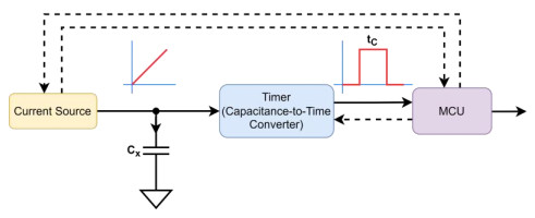
Currently, interdigital capacitive (IDC) sensors are widely used in science, industry and technology. To measure the changes in capacitance in these sensors, many methods such as differentiation, phase delay between two signals, capacitor charging/discharging, oscillators and switching circuits have been proposed. These techniques often use high frequencies and high complexity to measure small capacitance changes of fF or aF with high sensitivity. An analog interface based on a capacitance multiplier for capacitive sensors is presented. This study includes analysis of the interface error factors, such as the error due to the components of the capacitance multiplier, parasitic capacitances, transient effects and non-ideal parameters of OpAmp. A design approach based on an IDC sensor to measure the quality of edible oils is presented and implemented. The quality relates to the total polar compounds (TPC) and consequently to relative electrical permittivity
Citation: Vasileios Delimaras, Kyriakos Tsiakmakis, Argyrios T. Hatzopoulos. Analog interface based on capacitance multiplier for capacitive sensors and application to evaluate the quality of oils[J]. AIMS Electronics and Electrical Engineering, 2023, 7(4): 243-270. doi: 10.3934/electreng.2023015
Currently, interdigital capacitive (IDC) sensors are widely used in science, industry and technology. To measure the changes in capacitance in these sensors, many methods such as differentiation, phase delay between two signals, capacitor charging/discharging, oscillators and switching circuits have been proposed. These techniques often use high frequencies and high complexity to measure small capacitance changes of fF or aF with high sensitivity. An analog interface based on a capacitance multiplier for capacitive sensors is presented. This study includes analysis of the interface error factors, such as the error due to the components of the capacitance multiplier, parasitic capacitances, transient effects and non-ideal parameters of OpAmp. A design approach based on an IDC sensor to measure the quality of edible oils is presented and implemented. The quality relates to the total polar compounds (TPC) and consequently to relative electrical permittivity

| [1] |
Khan AU, Islam T, George B, Rehman M (2019) An Efficient Interface Circuit for Lossy Capacitive Sensors. IEEE Trans Instrum Meas 68: 829–836. https://doi.org/10.1109/TIM.2018.2853219 doi: 10.1109/TIM.2018.2853219

|
| [2] |
Wang L, Veselinovic M, Yang L, Geiss BJ, Dandy DS, Chen T (2017) A sensitive DNA capacitive biosensor using interdigitated electrodes. Biosens Bioelectron 87: 646–653. https://doi.org/10.1016/j.bios.2016.09.006 doi: 10.1016/j.bios.2016.09.006
|
| [3] |
Mahalingam D, Gurbuz Y, Qureshi A, Niazi JH (2015) Design, fabrication and performance evaluation of interdigital capacitive sensor for detection of Cardiac Troponin-Ⅰ and Human Epidermal Growth Factor Receptor 2. 2015 IEEE SENSORS - Proc 1–4. https://doi.org/10.1109/ICSENS.2015.7370209 doi: 10.1109/ICSENS.2015.7370209
|
| [4] |
Couniot N, Afzalian A, Van Overstraeten-Schlogel N, Francis LA, Flandre D (2016) Capacitive Biosensing of Bacterial Cells: Sensitivity Optimization. IEEE Sens J 16: 586–595. https://doi.org/10.1109/JSEN.2015.2485120 doi: 10.1109/JSEN.2015.2485120
|
| [5] |
Schaur S, Jakoby B (2011) A numerically efficient method of modeling interdigitated electrodes for capacitive film sensing. Procedia Eng 25: 431–434. https://doi.org/10.1016/j.proeng.2011.12.107 doi: 10.1016/j.proeng.2011.12.107
|
| [6] |
Senevirathna BP, Lu S, Dandin MP, Basile J, Smela E, Abshire PA (2018) Real-Time Measurements of Cell Proliferation Using a Lab-on-CMOS Capacitance Sensor Array. IEEE Trans Biomed Circuits Syst 12: 510–520. https://doi.org/10.1109/TBCAS.2018.2821060 doi: 10.1109/TBCAS.2018.2821060
|
| [7] |
Claudel J, Ngo TT, Kourtiche D, Nadi M (2020) Interdigitated Sensor Optimization for Blood Sample Analysis. Biosensors 10. https://doi.org/10.3390/bios10120208 doi: 10.3390/bios10120208
|
| [8] |
Meng J, Huang J, Oueslati R, Jiang Y, Chen J, Li S, et al. (2021) A single-step DNAzyme sensor for ultra-sensitive and rapid detection of Pb2+ ions. Electrochim Acta 368: 137551. https://doi.org/10.1016/j.electacta.2020.137551 doi: 10.1016/j.electacta.2020.137551
|
| [9] | Ramanathan P, Ramasamy S, Jain P, Nagrecha H, Paul S, Arulmozhivarman P, et al. (2013) Low Value Capacitance Measurements for Capacitive Sensors – A Review. Sensors & Transducers 148: 1–10. |
| [10] |
Ferlito U, Grasso AD, Pennisi S, Vaiana M, Bruno G (2020) Sub-Femto-Farad Resolution Electronic Interfaces for Integrated Capacitive Sensors: A Review. IEEE Access 8: 153969–153980. https://doi.org/10.1109/ACCESS.2020.3018130 doi: 10.1109/ACCESS.2020.3018130
|
| [11] |
Kanoun O, Kallel AY, Fendri A (2022) Measurement Methods for Capacitances in the Range of 1 pF–1 nF: A review. Measurement 195: 111067. https://doi.org/10.1016/j.measurement.2022.111067 doi: 10.1016/j.measurement.2022.111067
|
| [12] |
Forouhi S, Dehghani R, Ghafar-Zadeh E (2019) CMOS based capacitive sensors for life science applications: A review. Sensors Actuators, A Phys 297: 111531. https://doi.org/10.1016/j.sna.2019.111531 doi: 10.1016/j.sna.2019.111531
|
| [13] |
Preethichandra DMG, Shida K (2001) A simple interface circuit to measure very small capacitance changes in capacitive sensors. IEEE Trans Instrum Meas 50: 1583–1586. https://doi.org/10.1109/19.982949 doi: 10.1109/19.982949
|
| [14] |
Haider MR, Mahfouz MR, Islam SK, Eliza SA, Qu W, Pritchard E (2008) A low-power capacitance measurement circuit with high resolution and high degree of linearity. Midwest Symp Circuits Syst 261–264. https://doi.org/10.1109/MWSCAS.2008.4616786 doi: 10.1109/MWSCAS.2008.4616786
|
| [15] |
Dean RN, Rane A (2010) An improved capacitance measurement technique based of RC phase delay. 2010 IEEE Int Instrum Meas Technol Conf I2MTC 2010 - Proc 367–370. https://doi.org/10.1109/IMTC.2010.5488213 doi: 10.1109/IMTC.2010.5488213
|
| [16] |
Reverter F, Gasulla M, Pallàs-Areny R (2004) A low-cost microcontroller interface for low-value capacitive sensors. Conf Rec - IEEE Instrum Meas Technol Conf 3: 1771–1775. https://doi.org/10.1109/IMTC.2004.1351425 doi: 10.1109/IMTC.2004.1351425
|
| [17] |
Czaja Z (2020) A measurement method for capacitive sensors based on a versatile direct sensor-to-microcontroller interface circuit. Measurement 155: 107547. https://doi.org/10.1016/j.measurement.2020.107547 doi: 10.1016/j.measurement.2020.107547
|
| [18] |
Van Der Goes FML, Meijer GCM (1996) A novel low-cost capacitive-sensor interface. IEEE Trans Instrum Meas 45: 536–540. https://doi.org/10.1109/19.492782 doi: 10.1109/19.492782
|
| [19] |
Mohammad K, Thomson DJ (2017) Differential Ring Oscillator Based Capacitance Sensor for Microfluidic Applications. IEEE Trans Biomed Circuits Syst 11: 392–399. https://doi.org/10.1109/TBCAS.2016.2616346 doi: 10.1109/TBCAS.2016.2616346
|
| [20] |
Ashrafi A, Golnabi H (1999) A high precision method for measuring very small capacitance changes. Rev Sci Instrum 70: 3483–3487. https://doi.org/10.1063/1.1149941 doi: 10.1063/1.1149941
|
| [21] | Chatzandroulis S, Tsoukalas D (2001) Capacitance to frequency converter suitable for sensor applications using telemetry, ICECS'99. Proceedings of ICECS '99. 6th IEEE International Conference on Electronics, Circuits and Systems (Cat. No.99EX357), IEEE, 1791–1794. https://doi.org/10.1109/ICECS.1999.814557 |
| [22] |
Ramfos I, Chatzandroulis S (2012) A 16-channel capacitance-to-period converter for capacitive sensor applications. Analog Integr Circuits Signal Process 71: 383–389. https://doi.org/10.1007/s10470-011-9738-y doi: 10.1007/s10470-011-9738-y
|
| [23] |
Bruschi P, Nizza N, Dei M (2008) A low-power capacitance to pulse width converter for MEMS interfacing. ESSCIRC 2008 - Proc 34th Eur Solid-State Circuits Conf 1: 446–449. https://doi.org/10.1109/ESSCIRC.2008.4681888 doi: 10.1109/ESSCIRC.2008.4681888
|
| [24] |
Bruschi P, Nizza N, Piotto M (2007) A current-mode, dual slope, integrated capacitance-to-pulse duration converter. IEEE J Solid-State Circuits 42: 1884–1891. https://doi.org/10.1109/JSSC.2007.903102 doi: 10.1109/JSSC.2007.903102
|
| [25] |
Nizza N, Dei M, Butti F, Bruschi P (2013) A low-power interface for capacitive sensors with PWM output and intrinsic low pass characteristic. IEEE Trans Circuits Syst Ⅰ Regul Pap 60: 1419–1431. https://doi.org/10.1109/TCSI.2012.2220461 doi: 10.1109/TCSI.2012.2220461
|
| [26] |
Arefin MS, Redouté JM, Yuce MR (2016) A Low-Power and Wide-Range MEMS Capacitive Sensors Interface IC Using Pulse-Width Modulation for Biomedical Applications. IEEE Sens J 16: 6745–6754. https://doi.org/10.1109/JSEN.2016.2587668 doi: 10.1109/JSEN.2016.2587668
|
| [27] |
Lu JHL, Inerowicz M, Joo S, Kwon JK, Jung B (2011) A low-power, wide-dynamic-range semi-digital universal sensor readout circuit using pulsewidth modulation. IEEE Sens J 11: 1134–1144. https://doi.org/10.1109/JSEN.2010.2085430 doi: 10.1109/JSEN.2010.2085430
|
| [28] |
Brookhuis RA, Lammerink TSJ, Wiegerink RJ (2015) Differential capacitive sensing circuit for a multi-electrode capacitive force sensor. Sensors Actuators, A Phys 234: 168–179. https://doi.org/10.1016/j.sna.2015.08.020 doi: 10.1016/j.sna.2015.08.020
|
| [29] |
Tan Z, Shalmany SH, Meijer GC, Pertijs MA (2012) An energy-efficient 15-bit capacitive-sensor interface based on period modulation. IEEE J Solid-State Circuits 47: 1703–1711. https://doi.org/10.1109/JSSC.2012.2191212 doi: 10.1109/JSSC.2012.2191212
|
| [30] |
Li X, Meijer GCM (2002) An accurate interface for capacitive sensors. IEEE Trans Instrum Meas 51: 935–939. https://doi.org/10.1109/TIM.2002.807793 doi: 10.1109/TIM.2002.807793
|
| [31] |
Gasulla M, Li X, Meijer GCM (2005) The noise performance of a high-speed capacitive-sensor interface based on a relaxation oscillator and a fast counter. IEEE Trans Instrum Meas 54: 1934–1940. https://doi.org/10.1109/TIM.2005.853684 doi: 10.1109/TIM.2005.853684
|
| [32] |
Yurish SY (2009) Universal Capacitive Sensors and Transducers Interface. Procedia Chem 1: 441–444. https://doi.org/10.1016/j.proche.2009.07.110 doi: 10.1016/j.proche.2009.07.110
|
| [33] |
Heidary A, Meijer GCM (2009) An integrated interface circuit with a capacitance-to-voltage converter as front-end for grounded capacitive sensors. Meas Sci Technol 20. https://doi.org/10.1088/0957-0233/20/1/015202 doi: 10.1088/0957-0233/20/1/015202
|
| [34] |
Liu Y, Chen S, Nakayama M, Watanabe K (2000) Limitations of a relaxation oscillator in capacitance measurements. IEEE Trans Instrum Meas 49: 980–983. https://doi.org/10.1109/19.872917 doi: 10.1109/19.872917
|
| [35] |
Czaja Z (2023) A New Approach to Capacitive Sensor Measurements Based on a Microcontroller and a Three-Gate Stable RC Oscillator. IEEE Trans Instrum Meas 72: 1–9. https://doi.org/10.1109/TIM.2023.3244851 doi: 10.1109/TIM.2023.3244851
|
| [36] |
De Marcellis A, Reig C, Cubells-Beltrán M-D (2019) A Capacitance-to-Time Converter-Based Electronic Interface for Differential Capacitive Sensors. Electronics 8: 80. https://doi.org/10.3390/electronics8010080 doi: 10.3390/electronics8010080
|
| [37] |
Ulla Khan A, Islam T, Akhtar J (2016) An Oscillator-Based Active Bridge Circuit for Interfacing Capacitive Sensors with Microcontroller Compatibility. IEEE Trans Instrum Meas 65: 2560–2568. https://doi.org/10.1109/TIM.2016.2581519 doi: 10.1109/TIM.2016.2581519
|
| [38] |
Rahman O, Islam T, Khera N, Khan SA (2021) A Novel Application of the Cross-Capacitive Sensor in Real-Time Condition Monitoring of Transformer Oil. IEEE Trans Instrum Meas 70. https://doi.org/10.1109/TIM.2021.3111979 doi: 10.1109/TIM.2021.3111979
|
| [39] |
Khaled AY, Aziz SA, Ismail WIW, Rokhani FZ (2016) Capacitive sensing system for frying oil assessment during heating. Proceeding - 2015 IEEE Int Circuits Syst Symp ICSyS 2015 137–141. https://doi.org/10.1109/CircuitsAndSystems.2015.7394081 doi: 10.1109/CircuitsAndSystems.2015.7394081
|
| [40] | Khamil KN, Mood MAUC (2017) Dielectric sensing (capacitive) on cooking oil's TPC level. J Telecommun Electron Comput Eng 9: 27–32. |
| [41] |
Liu M, Qin X, Chen Z, Tang L, Borom B, Cao N, et al. (2019) Frying Oil Evaluation by a Portable Sensor Based on Dielectric Constant Measurement. Sensors: 1–11. https://doi.org/10.3390/s19245375 doi: 10.3390/s19245375
|
| [42] |
Kumar D, Singh A, Tarsikka PS (2013) Interrelationship between viscosity and electrical properties for edible oils. J Food Sci Technol 50: 549–554. https://doi.org/10.1007/s13197-011-0346-8 doi: 10.1007/s13197-011-0346-8
|
| [43] |
Pérez AT, Hadfield M (2011) Low-cost oil quality sensor based on changes in complex permittivity. Sensors 11: 10675–10690. https://doi.org/10.3390/s111110675 doi: 10.3390/s111110675
|
| [44] |
Behzadi G, Fekri L (2013) Electrical Parameter and Permittivity Measurement of Water Samples Using the Capacitive Sensor. Int J Water Resour Environ Sci 2: 66–75. https://doi.org/10.5829/idosi.ijwres.2013.2.3.2938 doi: 10.5829/idosi.ijwres.2013.2.3.2938
|
| [45] |
Golnabi H, Sharifian M (2013) Investigation of water electrical parameters as a function of measurement frequency using cylindrical capacitive sensors. Meas J Int Meas Confed 46: 305–314. https://doi.org/10.1016/j.measurement.2012.07.002 doi: 10.1016/j.measurement.2012.07.002
|
| [46] | Niranatlumpong P, Allen MA (2022) A 555 Timer IC Chaotic Circuit: Chaos in a Piecewise Linear System With Stable but No Unstable Equilibria. IEEE Trans Circuits Syst Ⅰ Regul Pap 69: 798–810. |


Figures(25) / Tables(4)

Vasileios Delimaras, Kyriakos Tsiakmakis, Argyrios T. Hatzopoulos. Analog interface based on capacitance multiplier for capacitive sensors and application to evaluate the quality of oils[J]. AIMS Electronics and Electrical Engineering, 2023, 7(4): 243-270. doi: 10.3934/electreng.2023015


 DownLoad: