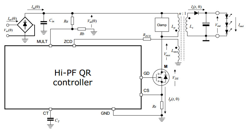
Figure 1.
Principle schematic of an LED driver based on a Hi-PF QR flyback converter.
Citation: Giovanni Gritti, Claudio Adragna. Analysis, design and performance evaluation of an LED driver with unity power factor and constant-current primary sensing regulation[J]. AIMS Energy, 2019, 7(5): 579-599. doi: 10.3934/energy.2019.5.579
| [1] | Anthoula Menti, Dimitrios Barkas, Pavlos Pachos, Constantinos S. Psomopoulos . Contribution of a power multivector to distorting load identification. AIMS Energy, 2023, 11(2): 271-292. doi: 10.3934/energy.2023015 |
| [2] | Nagaraj C, K Manjunatha Sharma . Fuzzy PI controller for bidirectional power flow applications with harmonic current mitigation under unbalanced scenario. AIMS Energy, 2018, 6(5): 695-709. doi: 10.3934/energy.2018.5.695 |
| [3] | Pascal Hategekimana, Adrià Junyent-Ferré, Etienne Ntagwirumugara, Joan Marc Rodriguez Bernuz . Improved methods for controlling interconnected DC microgrids in rural villages. AIMS Energy, 2024, 12(1): 214-234. doi: 10.3934/energy.2024010 |
| [4] | Dimitrios Barkas, Anthoula Menti, Pavlos Pachos, Constantinos S. Psomopoulos . Experimental investigation of the impact of environmental parameters on the supraharmonic emissions of PV inverters. AIMS Energy, 2024, 12(4): 761-773. doi: 10.3934/energy.2024036 |
| [5] | K. M. S. Y. Konara, M. L. Kolhe, Arvind Sharma . Power dispatching techniques as a finite state machine for a standalone photovoltaic system with a hybrid energy storage. AIMS Energy, 2020, 8(2): 214-230. doi: 10.3934/energy.2020.2.214 |
| [6] | Ivan Ramljak, Amir Tokić . Harmonic emission of LED lighting. AIMS Energy, 2020, 8(1): 1-26. doi: 10.3934/energy.2020.1.1 |
| [7] | Andrey Dar'enkov, Aleksey Kralin, Evgeny Kryukov, Yaroslav Petukhov . Research into the operating modes of a stand-alone dual-channel hybrid power system. AIMS Energy, 2024, 12(3): 706-726. doi: 10.3934/energy.2024033 |
| [8] | Armando L. Figueroa-Acevedo, Michael S. Czahor, David E. Jahn . A comparison of the technological, economic, public policy, and environmental factors of HVDC and HVAC interregional transmission. AIMS Energy, 2015, 3(1): 144-161. doi: 10.3934/energy.2015.1.144 |
| [9] | Rasool M. Imran, Kadhim Hamzah Chalok . Innovative mode selective control and parameterization for charging Li-ion batteries in a PV system. AIMS Energy, 2024, 12(4): 822-839. doi: 10.3934/energy.2024039 |
| [10] | Akash Talwariya, Pushpendra Singh, Mohan Lal Kolhe, Jalpa H. Jobanputra . Fuzzy logic controller and game theory based distributed energy resources allocation. AIMS Energy, 2020, 8(3): 474-492. doi: 10.3934/energy.2020.3.474 |
The design of LED drivers is challenging in many respects [1]. For circuits supplied from the ac power line, the harmonic content of the ac input current is a relevant demanding aspect.
Due to the proliferation of LED lamps, the effect of low/medium power LED drivers on the electric power distribution line is a major concern [2,3,4]. For this reason, these systems must comply with the class C harmonic emission limits defined by the IEC61000-3-2 or other equivalent regulations. In addition, market requirements put considerable emphasis on the Total Harmonic Distortion (THD) of the ac input current: LED drivers are quite often specified to meet THD targets [5,6,7,8,9] that turn out to be more severe than the regulatory requirements of IEC61000-3-2 on the amplitude of the individual harmonics.
Standalone LED drivers (i.e., not embedded into a luminaire) are particularly challenging in this respect: they are often specified for a rated output current over a range of output voltages (a 2:1 range is quite typical) to power different types/lengths of LED strings. These devices must then comply with the IEC61000-3-2 and meet the THD targets even when operated at the specified minimum output voltage, which means at a fraction of their rated maximum power. To make things worse, in many cases light emission must be dimmable and/or drivers are specified to operate over a wide input voltage range (from 90 to 264 Vac). From the driver perspective, these features further extend the input voltage and the power range under consideration for THD targets.
From a different angle, LED drivers are a cost-sensitive application and quite a common way to help meet cost targets is to use the so-called constant-current primary sensing regulation (CC-PSR) technique. This configuration regulates the output dc current required for proper LED driving using only electrical quantities available on the primary side. In this way, the current sensing element, the voltage reference, the error amplifier on the secondary side and the optocoupler that transfers the error signal to the control circuit on the primary side are unnecessary. In addition to reducing the bill of materials and the required board space, this approach brings greater safety and reliability.
The high-power-factor (Hi-PF) flyback converter is perhaps the most popular topology used in low/medium power LED drivers supplied from the ac power line [10,11,12,13,14,15,16,17,18,19,20,21,22,23,24,25]. It meets the regulatory requirements on the power factor and the ac input current harmonic content, as well as those on safety isolation, with a simple and inexpensive power stage. Additionally, it lends itself to implementing CC-PSR in a relatively simple way and with good performance [15,16,17,18,19,20,21,22].
In many cases, Hi-PF flyback converters are operated with a fixed switching frequency and in the discontinuous conduction mode (FF-DCM) [10,11,12,13,14,15,16,17,18]. As taught in [26], this makes the flyback converter an ideal rectifier, theoretically able to provide unity power factor and zero THD.
Hi-PF flyback converters can also be operated in the so-called QR mode, i.e., synchronizing the beginning of switching cycles to transformer demagnetization. QR operation brings a few benefits as compared to FF-DCM: lower conducted EMI emissions, safer operation under short circuit conditions, valley-switching or even true soft-switching (zero-voltage switching, ZVS). However, its standard implementation (that can be found in a large number of commercial products primarily intended for boost PFC converters) provides a sinusoidal envelope of the peaks of the primary current. This cannot achieve a very low THD of the input current, as demonstrated in [19,20,21,22,23,24,25]. In these papers, various techniques to reduce the THD are reported. Though effective, none of them can theoretically provide unity power factor and zero THD like in a FF-DCM Hi-PF flyback converter.
Relatively recently, a control method has been disclosed [27] that is able to provide Hi-PF QR flyback converters, whose basic circuit is shown in Figure 1, with the ability to ideally get a sinusoidal input current (unity power factor and zero THD like FF-DCM ones) and to perform CC-PSR. In this way, the combined benefits of QR operation and CC-PSR can be obtained with minimum penalty in terms of THD. The present work will take this method under consideration.
The analysis presented in the existing literature on this topic [27,28], however, does not fully explore the causes of distortion of the input current that are inherent in the control method. This will be the main focus of the present work, with the aim of providing some design guidelines to meet the THD design targets with less effort. Therefore, this paper is arranged as follows: in section 2 the method [27] is reviewed; section 3 reviews the basic assumptions underlying the method, deals with the causes of distortion of the input current not previously analyzed and provides a few design guidelines to achieve minimum THD of the input current; section 4 will show some experimental results that validate the analysis; section 5 provides the conclusions.
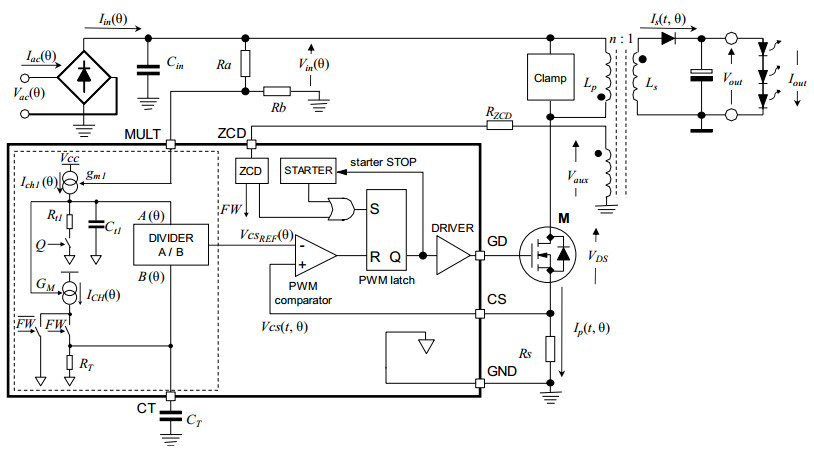
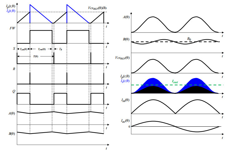
The control method described in [27] is essentially the combination of the control scheme described in [28] that ideally achieves a sinusoidal input current in a Hi-PF QR flyback converter with secondary-side regulation, and that described in [29] that achieves CC-PSR in a traditionally controlled Hi-PF QR flyback converter. Figure 2 shows the principle schematic, Figure 3 its key waveforms.
Basically, with the first method the peaks of the primary current are enveloped by a properly shaped profile so that the average input current in a switching cycle tracks exactly the profile of the rectified input voltage. With the second method, the amplitude of the peaks is controlled in a way that the average output current on a line cycle time base is kept constant.
Recalling [27], the rectified input current to the converter, Iin(θ), with (0 < θ < π), which is found by averaging the primary current over each switching cycle, has the following expression:
| Iin(θ)=12Ipkp(θ)TON(θ)T(θ) | (1) |
The peak envelope of the primary current Ipkp(θ) is determined by the programmed current reference VcsREF(θ) through the current sensing resistors RS:
| Ipkp(θ)=VcsREF(θ)Rs | (2) |
Therefore, to achieve a sinusoidal ac input current Iac(θ), with (0 < θ < 2π), which is the odd counterpart of Iin(θ), VcsREF(θ) must be of the following type:
| VcsREF(θ)=VcsxsinθT(θ)TON(θ) | (3) |
With reference to the control circuit in Figure 2, VcsREF(θ) is the output of an analog divider where its input A(θ) can be identified as the output of the shaper circuit (composed by Rt1, Ct1, Ich1 and switch driven by the timing signal Q) needed to achieve the sinusoidal input current [28]; its input B(θ) signal can be considered constant and is generated (through RT, CT, ICH and the transformer demagnetization FW timing signal) in a proper way to achieve output current regulation [29].
With the same assumptions as in [28], applying charge balance to Ct1 the resulting A(θ) signal is:
| A(θ)=Rt1Ich1(θ)T(θ)TON(θ)=Rt1gm1Kp(VPKsinθ)T(θ)TON(θ) | (4) |
where gm1 is the current-to-voltage gain of the current generator Ich1(θ), VPK the peak of the rectified line voltage Vin(θ) and Kp the divider ratio Rb/(Ra + Rb). Applying charge balance to CT and denoting with GM the current-to-voltage gain of the current generator ICH(θ), it is possible to find:
| B(θ)=GMRTgm1Rt1Kp(VPKsinθ)TFW(θ)TON(θ) | (5) |
CT is assumed to be large enough so that the ac component (at twice the line frequency fL) of B(θ) is negligible with respect to its dc component B0:
| B0=¯B(θ)=1πGMRTgm1Rt1KpVPKπ∫0sinθTFW(θ)TON(θ)dθ | (6) |
Applying the voltage-second balance to the primary winding of the flyback transformer, the on-time TON(θ) of the power switch M and the secondary conduction time TFW(θ) are related by the following relationship:
| (VPKsinθ)TON(θ)=n(Vout+VF)TFW(θ)=VRTFW(θ) | (7) |
Considering that Kv = VPK/VR, the ratio between the times TFW (θ) and TON (θ) is:
| TFW(θ)TON(θ)=Kvsinθ | (8) |
The dc component B0 of B(θ) is found by combining (8) and (6) and solving the integral:
| B0=GMRTgm1Rt1KpVPKKv2 | (9) |
Finally, the current reference VcsREF(θ), output of the divider A/B, is:
| VcsREF(θ)=KDA(θ)B(θ)≈KDA(θ)B0=2KDGMRTKvsinθT(θ)TON(θ) | (10) |
where KD is the divider gain (dimensionally a voltage).
Equation 10 has the same form as (3), with Vcsx = 2 KD/(GM RT Kv), thus the control mechanism in Figure 2 shapes the rectified input current Iin(θ) as a rectified sinusoid and, then, the ac input current Iac(θ) as a sinusoid. It is worth noticing that this result is achieved independently from the duration TR of the time interval following transformer demagnetization (refer to Figure 3). The only constraint is that the converter does not operate in CCM (Continuous Conduction Mode).
The peak envelope of the secondary current Ipks(θ) can be calculated considering that the secondary current is n = Np/Ns times the primary current Ipkp(θ), found by combining (10) and (2):
| {Ipkp(θ)=1RS2KDGMRTKvsinθT(θ)TON(θ)Ipks(θ)=nRS2KDGMRTKvsinθT(θ)TON(θ) | (11) |
The average value in a switching cycle of the secondary current is:
| Io(θ)=12Ipks(θ)TFW(θ)T(θ)=1RSnKDGMRTKvsinθTFW(θ)TON(θ) | (12) |
and the dc output current Iout is the average of Io(θ) over a line half-cycle:
| Iout=¯Io(θ)=1ππ∫0nKDGMRTKvRSsinθTFW(θ)TON(θ)dθ | (13) |
Finally, combining (13) and (8) and solving the integral the average output current is given by:
| Iout=nKD2GMRTRS | (14) |
which shows that the regulated dc output current Iout depends solely on external, user-selectable parameters (n, Rs) and on internally fixed parameters (GM, RT, KD). It does not depend on the output voltage Vout, nor on the rms input voltage Vin or the switching frequency fSW (θ) = 1/T(θ).
Therefore, the control circuit shown in Figure 2, in addition to providing ideally unity power factor and zero harmonic distortion of the ac input current (PF = 1 and THD = 0), performs CC-PSR as well, i.e., it provides a regulated output current using only quantities available on the primary side, without any dedicated circuitry on the secondary side.
It is worth noticing that also the ability to perform CC-PSR is constrained to the converter not operating in CCM.
In this section the discussion will be focused on the sinusoidal shaping of the input current operated by the control method analyzed in the previous section. As highlighted in [27,28,29], this analysis is based on some fundamental assumptions. Specifically:
1.The converter is operated so that the power switch M is turned on in each cycle after the secondary current reaches zero, therefore in QR-mode (i.e., on the first valley of the ringing that follows secondary current zeroing) or DCM (Discontinuous Conduction Mode).
2.The line voltage is sinusoidal, the input bridge rectifier is ideal, the voltage drop across the power switch M in the ON-state is negligible and there is negligible energy accumulation on the dc side of the bridge, thus the voltage Vin(θ), sensed by the (Ra, Rb) divider and used as a 'template' for the input current shape, is a rectified sinusoid.
3.The transformer's windings are perfectly coupled (no leakage inductance), so that the energy stored in the primary winding is instantaneously transferred to the secondary winding; further, the turn-off transient of the power switch M has negligible duration. As a result, TFW immediately follows TON.
In addition, achieving a sinusoidal shape of Iac(θ) is based on the following assumptions inherent in (1) and (10) respectively:
4.During the time interval TR elapsing from the instant when the transformer demagnetizes to the instant when the power switch M is turned on, the transformer current is constantly zero; consequently, the current in the instant when M is turned on is zero too (Zero-current switching at turn-on, ZCS).
5.the ac component (at twice the line frequency fL) of the control voltage B(θ) is negligible with respect to its dc component B0, like in any high-PF converter;
Assumption 1 is actually a constraint, already discussed in [28]: if not met, the system will not operate as expected. The other assumptions are approximations that simplify the analysis and, as such, may lead to overlooking phenomena that cause distortion of the input current. Assumptions 2, 3 and 4 actually concern the power processing mechanism of the Hi-PF QR flyback converter and their impact on the distortion of the input current will be addressed in another paper.
In this section the focus is on the causes of distortion ascribable to the control method. Some of them (switching frequency voltage ripple across the shaping capacitor Ct1, actual low-frequency shape of the reference generated across Ct1 and propagation delay on the current sense path) have been analyzed in [28] already and will not be treated here. The discussion in this section will concentrate on the implications of assumption 5, which is crucial for the selection of the capacitor CT (a selection criterion is missing so far); additionally, the effects of the input offset voltage of the PWM comparator (see Figure 2) will be investigated with the aim of providing a design criterion to the IC designer.
3.1 Distortion caused by the low frequency ripple of the control voltage B(θ)
The ac component at 2fL of the control voltage B(θ), though small as compared to its dc component B0, is a source of distortion inherent in the control method. To evaluate its impact, it is convenient to rewrite (5) taking (8) into account and simplifying the notation:
| B(θ)=Γsin2θ=Γ2(1−cos2θ) | (15) |
It is easy to recognize that Γ/2 = B0. This equation is the result of averaging over a switching cycle; in other words, it expresses the voltage that would be developed across the resistor RT if the CT capacitor (see Figure 2) was just large enough to make the ac component at the switching frequency negligible. However, in order for assumption 5 to be valid, CT must be much bigger, in order to keep the ac component at 2 fL low as well.
It is possible to think that B(θ) given by (15) is obtained by an equivalent current generator B(θ)/RT, whose dc and ac component are both equal to Γ/2RT = B0/RT. As we consider a large capacitor CT in parallel to RT, so that its reactance XT at f = 2 fL is much smaller than RT, the dc component B0/RT develops the dc voltage B0 while the ac component B0/RT generates an ac voltage in quadrature (lagging) whose peak amplitude Bacpk is equal to B0 XT/RT:
| B(θ)=B0(1−14πfLRTCTsin2θ) | (16) |
Substituting this expression in (10) and taking (2) into account, (1) can be rewritten as:
| Iin(θ)=12VcsxRssinθ1−14πfLRTCTsin2θ | (17) |
Iac(θ) is given by (17) too, simply considering θ ∈ (0, 2π).
The diagrams in Figure 4, left to right, show the shape of Iac(θ) for increasing values of the quantity (4πfL RT CT)-1 i.e., for increasing amplitude of the low frequency ac component of B(θ) (compared to the dc value B0). A dotted black sinusoid is shown too for reference.
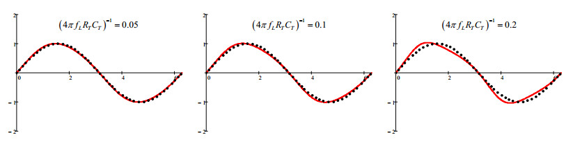
A Fourier analysis of (17) shows that there is an additional small component at the fundamental frequency and that the distortion is nearly all concentrated on the third harmonic; the higher order odd harmonics (even harmonics are zero, being the function hemisymmetrical) become negligible very quickly, as depicted in the left-hand diagram of Figure 5.
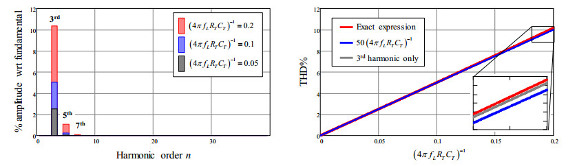
The Fourier series expansion of (17) involves both sines and cosines, so that the odd harmonics are alternately in-phase and in quadrature with the fundamental. In particular, the fundamental leads sin(θ) by few degrees and the third harmonic lags behind the fundamental by 90°.
The THD of the input current resulting from (17) is shown in the right-hand diagram of Figure 5 (red trace) along with its approximate expression (blue trace):
| THD%=504πfLRTCT | (18) |
which provides a simple and accurate relationship linking the amount of distortion generated by the low-frequency ripple on the control voltage and the capacitor CT. In fact, the error is < 0.5% for values of (4πfL RT CT)-1 within 0.2 and < 0.13% for values of (4πfL RT CT)-1 within 0.1.
The plot on the right-hand side of Figure 5 shows also the 3rd harmonic (grey trace), visible in the zoomed window only, which is essentially overlapped to the THD plot, reiterating the dominance of the third harmonic: it accounts for 99.5% of THD at (4πfL RT CT)-1 = 0.2 and for 99.9% of THD at (4πfL RT CT)-1 = 0.1.
Notice that (18) can be rewritten as:
| THD%=50BacpkB0 | (19) |
This is essentially equal to the expression of the third-harmonic distortion that can be found for multiplier-based power factor correction schemes [30]. This proves that using an analog divider instead of the multiplier does not bring any significant difference in terms of input current distortion as long as the peak amplitude of the ac component of B(θ), Bacpk, is sufficiently smaller than the dc component B0. To confirm this statement from a different angle, it is possible to prove that, expanding (17) to Maclaurin series with respect to the variable (4πfL RT CT)-1, the first order term is exactly the same that is found in case of multiplier-based power factor correction schemes.
In principle, once specified the 3rd harmonic distortion budget allocated to the low-frequency ripple, either (18) or (19) enable the computation of the required CT value. In section 4 a more practical design rule will be provided; based on that, the required CT value can be computed with (16).
It is well-known that the input offset voltage of a comparator is the differential input voltage at which its output changes from one logic level to the other. It is most often caused by the mismatch of the transistors (either BJTs or FETs) in the input stage. These transistors should be relatively large to minimize the causes of mismatch but large transistors are slower (and more silicon consuming!) than small transistors. On the other hand, the PWM comparator (see Figure 2) must be fast to minimize the total propagation delay in the current sense path. For this reason, in commercially available control ICs the offset of the PWM comparator is the result of a trade-off.
Usually the offset is in the 10 mV range, a voltage level that in any PFC converter is found on the current sense input when the line voltage is around the zero crossings. It is therefore worth investigating its effect on the shape of the input current.
Input offset voltage is symbolically represented by a voltage source in series with either input terminal of the comparator. In our analysis it is convenient to consider this generator so that it adds up to the VcsREF(θ) signal, as shown in Figure 6. Notice that Vo can be either positive or negative. With this representation, the turn-off condition (2) of the power switch M can be rewritten as:
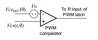
| Ipkp(θ)=VcsREF(θ)+VoRs | (20) |
where VcsREF(θ) is still given by (3). This considering, (1) becomes:
| Iin(θ)=12Rs[Vcsxsinθ+VoTON(θ)T(θ)] | (21) |
The contribution of the input offset voltage, expressed by the term Vo TON(θ)/T(θ) in (21), has a twofold effect: on the one hand it offsets (upwards or downwards, depending on the sign of Vo) the input current waveform, like with the traditional control technique, producing crossover distortion; on the other hand, since the actual offset is a function of the instantaneous line voltage (because of the term TON(θ)/T(θ)), the shape of the current is affected as well. The amount of distortion caused by the offset Vo depends on the ratio Vo/Vcsx and a Fourier analysis of (21) shows that the distortion term creates a component at the fundamental frequency and odd harmonics, all in-phase (if Vo > 0) or 180° out of phase (if Vo < 0) with the fundamental component (no cosine term involved, then).
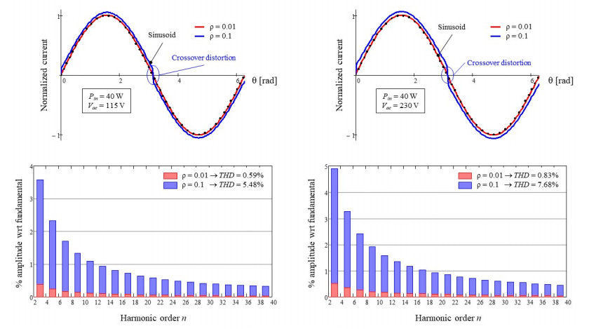
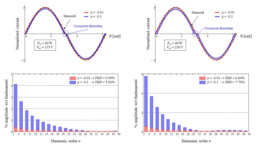
The diagrams of Figures 7 and 8 provide some exemplary quantitative results for the converter specified in Table 1, considering a positive and a negative offset respectively. The calculation method used to obtain these results is clarified in the appendix. The input offset is represented by the parameter ρ = Vo/Vcsx-max, where Vcsx-max is the maximum value of Vcsx = 2 KD /(GM RT Kv), i.e., the one corresponding to the minimum value of Kv, Kv-min = VPK-min/VR).
| Parameter | Symbol | Value | Unit |
| Line voltage range | Vacmin-Vacmax | 90–264 | Vac |
| Line frequency range | fl | 47–63 | Hz |
| Rated output voltage (14 LED string @ 100% load) | Vout | 48 | V |
| Regulated dc output current | Iout | 700 | mA |
| Expected full-load efficiency | η | 84 | % |
| Transformer primary inductance | Lp | 500 | μH |
| Reflected voltage | VR | 120 | V |
| Drain node total capacitance | CDS | 150 | pF |
 DownLoad:
CSV
DownLoad:
CSV
Notice that in LED drivers specified to work in a certain range of output voltages Vout to power different types/lengths of LED strings, VR is also variable, as stated by (7). Therefore, Kv is minimum at the upper end of the Vout range and maximum at the lower end of the Vout range. Notice also that in a CC-regulated converter a lower Vout (and VR) means also a lower output (and input) power.
In both Figures 7 and 8, the diagrams on the left-hand side are relevant full load and Vac = 115 V, those on the right-hand side are relevant to full load and Vac = 230 V. The upper diagrams show the shape of the ac input current to the converter Iac(θ) for two different values of ρ:ρ = 0.01 is realistic, ρ = 0.1 is exaggerated but has been considered to show more clearly the distortion caused. Currents are normalized to their peak value. A dotted black sinusoid is shown too for reference. The lower diagrams show the harmonic contents of the current waveforms in the upper diagrams.
Notice in Figure 7 that the shape of Iac(θ) shows a little crossover distortion, highlighted by the blue circle, i.e., a sort of step change in Iac(θ) from positive to negative and vice versa at the zero crossings of the instantaneous line voltage Vac(θ). This is due to the positive offset that keeps the average input current larger than zero even with an extremely small Vin(θ). This distortion is essentially invisible for ρ = 0.01, quite conspicuous for ρ = 0.1 and this is confirmed by the harmonic contents of Iac(θ) and the resulting values of THD.
In Figure 8, which refers to the case of a negative input offset voltage, the shape of Iac(θ) shows a different type of crossover distortion, highlighted by the blue circle: a time interval around zero crossings of the instantaneous line voltage Vac(θ) where Iac(θ) = 0, although Vac(θ) ≠ 0.
This type of crossover distortion, often termed dead zone, occurs when the term in brackets in (21) is negative. The physical interpretation of being Iin(θ) < 0 and Iac(θ) = 0 around zero-crossings is that a negative Iin(θ) actually charges back the input capacitor (Cin in Figure 2) so that Vin(θ) becomes larger than Vac(θ), the input bridge is reverse-biased and, consequently, Iac(θ) is zero. Also in this case the distortion is negligible for ρ = 0.01 and conspicuous for ρ = 0.1. The harmonic contents and THD values are only slightly larger than in the case of positive offset, hence one could conclude that, apart from the different shape, a positive offset or a negative offset are essentially equivalent in terms of input current shape degradation.
However, there are very good reasons that make a positive offset preferable to a negative one. There are a number of phenomena related to the power processing mechanism of Hi-PF QR flyback converters, specifically those neglected by the previously mentioned simplifying assumptions 2, 3 and 4, that produce a dead zone in the ac input current Iac(θ) like a negative offset. An additional negative offset would then exacerbate these phenomena, whereas a positive offset counteracts them and mitigates their effect.
The solutions described in [30], where these phenomena are described with reference to boost topology, are based on this concept.
As a conclusion, it is possible to state that as long as input offset voltage Vo is in the range of 1% of the dynamics of the current sense input, its contribution to the THD of the input current is extremely limited (well below 1%). Normally, the dynamics of the current sense input is dictated by considerations about the power dissipation on the sense resistor Rs, and the offset should be designed consequently. Conversely, if for any reasons the PWM comparator can be built with a given maximum Vo, say 10 mV, the dynamics of the current sense input should not be much lower than 1 V.
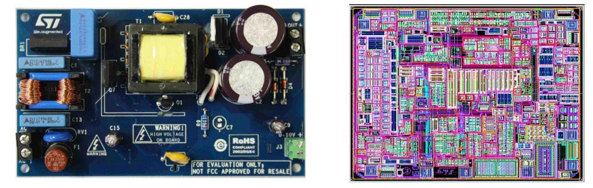
A prototype of an LED driver, shown in Figure 9 on the left-hand side and based on the reference Hi-PF QR flyback converter specified in Table 1, has been built and its performance evaluated on the bench. The control method reviewed in section 2 has been implemented in a test chip, shown in Figure 9 on the right-hand side, using STMicroelectronics' BCD6s (0.32 µm) technology.
Figures 10 to 12 summarize the salient results of this evaluation.
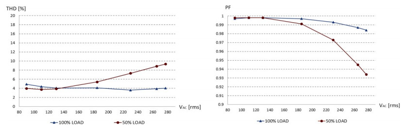
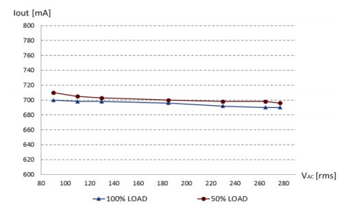
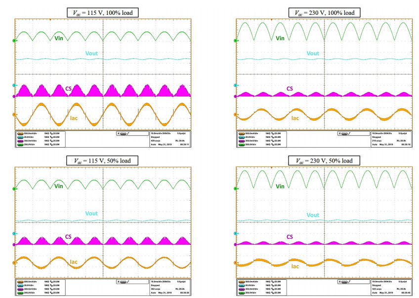
Figure 10 shows the values of THD and PF achieved under different loading conditions over the full input voltage range. The THD is around 4% over the input voltage range. At 50% load (same output current, half the output voltage) it is still close to 4% at low line and increases at high line, reaching 7.3% at 230 Vac and remaining below 10% at the upper end of the operating range. The PF is greater than 0.98 over the input voltage range at 100% load; at 50% load, at low line it is nearly equal to that at 100% load, at high line it drops to about 0.97 at 230 Vac.
The plot of Figure 11 shows the output current regulation versus ac line voltage (i.e., the dc current delivered to the LED string), for different LED string voltages. The regulated output current Iout, determined by the CC-PSR mechanism, lies in a band of ±10 mA centered on the target setpoint (700 mA, therefore ±1.4%), over the ac line voltage range and from 50% to 100% load. For a fixed load, the regulation band is approximately half as much. These measurements prove the very good accuracy of the CC-PSR regulation algorithm.
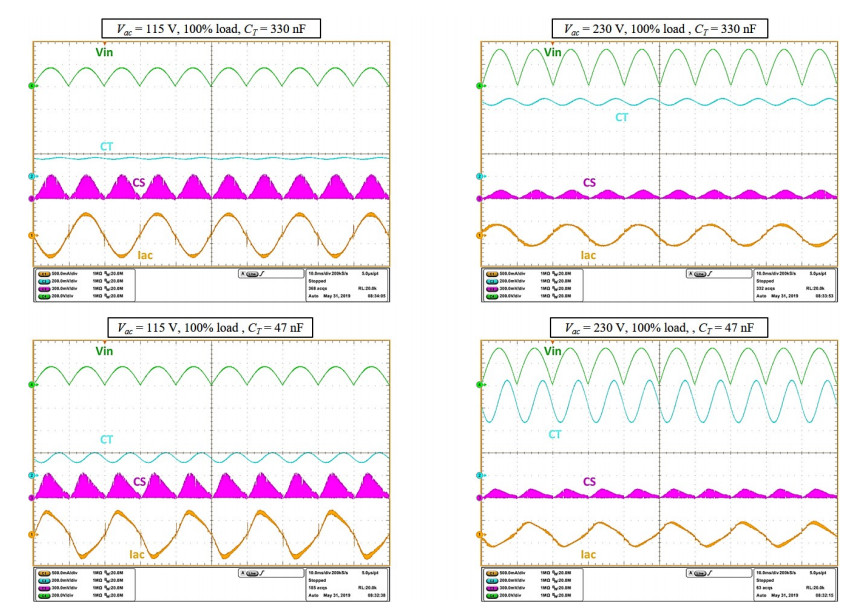
The experimental waveforms in Figure 12 show a shape if Iac(θ) that is very close to an ideal sinusoid at full load both at 115 Vac and 230 Vac. At half load and 115 Vac the waveform is still very close to a sinusoid, whereas at 230 Vac the distortion, though low, is clearly visible. Notice that at full load and 115 Vac Iac(θ) shows spikes at the zero crossings. These are due to the low frequency operation of the converter that comes close to the resonance frequency of the EMI filter. However, the harmonic contribution of these spikes are confined in the high frequency region, typically above the 40th harmonic considered by the regulations on harmonic current emissions (e.g., IEC61000-3-2).
Next, the dependence of the THD of Iac(θ) on the value of the capacitor CT was explored.
All the data and waveforms shown in Figures 10 to 12 are taken with CT = 330 nF. In the control IC it is RT = 120 kΩ, then (4πfL RT CT)-1 = 0.04 with fL = 50 Hz (this line frequency has been used throughout all measurements); the value of CT was swept in the range from 330 nF down to 22 nF, so that (4πfL RT CT)-1 changed in the range 0.04 to 0.603, and the value of THD measured at full load and different input voltages. The results are summarized in the plot of Figure 13.
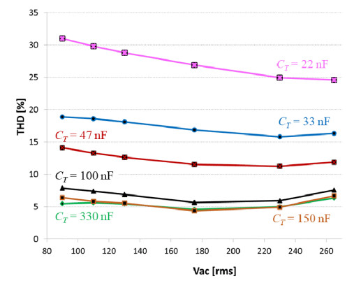
The results obtained with CT = 150 nF, corresponding to (4πfL RT CT)-1 = 0.088, are essentially coincident with those with CT = 330 nF, except at 90 Vac where the THD is about 1% higher.
With CT = 100 nF, i.e., (4πfL RT CT)-1 = 0.133, THD values increase by about 1–1.5% over those with CT = 150 nF, still remaining well below 10% over the input voltage range. Significant degradation of THD can be observed with CT values of 47 nF, corresponding to (4πfL RT CT)-1 = 0.282, and below. The experimental waveforms in Figure 14 refer to this condition.
From these results it is possible to conclude that, as long as (4πfL RT CT)-1 < 0.1, the THD of Iac(θ) does not change much with CT (its tolerance, as well as that of RT, has little effect, then); additionally, there is no significant benefit in going below (4πfL RT CT)-1 < 0.05; rather, since this involves larger CT values and the larger CT is, the slower is the response of the CC-PSR loop to line and load changes, a design target of (4πfL RT CT)-1 = 0.1 seems an educated choice.
In other words, considering (16), the system designer should target a peak amplitude of the ac ripple of B(θ), Bacpk, equal to 10% of its dc value B0, i.e., (4πfL RT CT)-1 ≤ 0.1. Since it is RT = 120 kΩ, the value of CT can be easily derived. Then, THD performance and dynamic performance can be traded off against one another to find the overall optimum operation with a series of bench tests.
The control methodology proposed in [27] that enables Hi-PF QR flyback converters with peak current mode control to ideally draw a sinusoidal current from the input source while regulating the output current using only quantities available on the primary side of the converter has been reviewed. After explaining the operating principle, the fundamental equations describing its operation have been recalled. A noticeable characteristic of the methodology emerging from this review is its user-friendliness: only two external parts are needed to set up a converter: a capacitor (CT) to optimize the ac input current shape, and a resistor (Rs) to set the regulated output current.
The subsequent discussion has been concentrated on the effects of some significant nonidealities that in the real-world operation adversely affect the THD of the input current that were not previously analyzed. Specifically, the effects of the low frequency ac ripple on the control voltage of the CC-PSR loop (which the selection of the tuning element CT depends on) and of the input voltage offset of the PWM comparator have been addressed.
The result of this analysis, corroborated by the experiments carried out on a prototype of an exemplary LED driver based on a control IC that implements the methodology under discussion, can be synthesized in the following two points:
1.The IC designer should target a ratio between the input voltage offset Vo of the PWM comparator and the dynamics of the current sense signal Vcsx-max not exceeding 1%. In most practical cases the value of Vcsx-max is dictated by considerations on the power dissipation of the current sensing resistor Rs and the effort directed to keeping Vo within that limit. Ideally, measures should be taken to achieve an always positive Vo because this would mitigate the effects of other nonidealities present in the system.
2.The system designer should target a peak amplitude of the ac ripple in the control voltage B(θ), Bacpk, equal to 10% of its dc value B0 as a starting point for experimental system optimization. Being the Bacpk/B0 ratio equal to the quantity (4πfL RT CT)-1, this is done through a proper selection of the CT capacitor. This choice typically ensures an acceptable THD level that is also little sensitive to the tolerance of CT. The optimum value of CT will be found experimentally trading off the THD performance against the dynamic performance in case of line/load changes.
Of course, in the design of an LED driver, there are additional design guidelines to be taken into consideration to optimize the THD of the input current throughout the operating range. As mentioned in the preliminary discussion of the control method, in addition to the nonidealities in the control there are nonidealities in the power processing mechanism of the Hi-PF QR flyback converter that cause distortion of the input current. The most significant ones are the negative current after demagnetization, the zero-current detection mechanism, the input capacitor after the bridge rectifier.
Their impact can be minimized with proper design choices, but this is the topic of a future work.
Firstly, it is convenient to rewrite (21) as follows:
| Iin(θ)=Vcsx2Rs[sinθ+VoVcsxTON(θ)T(θ)] | (A1) |
Introducing the parameter ρ = Vo/Vcsx-max, and keeping in mind the definitions of Vcsx, Vcsx-max given in section 3.2, (A1) can be expressed as:
| Iin(θ)=Vcsx2Rs[sinθ+ρKvKv−minTON(θ)T(θ)] | (A2) |
It is now necessary to calculate the ratio TON(θ)/T(θ). In [28] one can find an approximate expression of TON(θ)/T(θ) that neglects the idle time TR after transformer demagnetization and before the beginning of a new switching cycle (refer to Figure 3). Here we want to provide a more accurate expression that takes TR into account and that is used to build the plots of Figures 7 and 8.
The basic definition of T(θ), T(θ) = TON(θ) + TFW(θ) + TR, by virtue of (8) becomes:
| T(θ)=TON(θ)(1+Kvsinθ)+TR | (A3) |
As demonstrated in [28], the quantity TON2(θ)/T(θ) is constant for assigned operating conditions and its value is:
| T2ON(θ)T(θ)=4LpK2vV2RPin | (A4) |
By combining (A3) and (A4) it is possible to obtain the following quadratic equation in TON(θ):
| T2ON(θ)−4LpPinK2vV2R(1+Kvsinθ)TON(θ)−4LpPinK2vV2RTR=0 | (A5) |
The solution is:
| TON(θ)=2KvVR{LpPinVR1+KvsinθKv+√LpPin[LpPinV2R(1+KvsinθKv)2+TR]} | (A6) |
Of course, T(θ) is obtained inserting (A6) in (A3), and the ratio TON(θ)/T(θ) can be readily computed using Mathcad® or other similar calculation tool. It is possible to recognize that, if in (A6) we set TR = 0, then we find again the expressions of TON(θ) and T(θ) provided in [28].
The author declares no conflicts of interest in this paper.
| [1] | Lasance CJM, Poppe A (2014) Thermal Management for LED Applications. New York: Springer. |
| [2] | Uddin S, Shareef H, Mohamed A, et al. (2012) Harmonics and thermal characteristics of low wattage LED lamps. Przegl Elektrotech 88: 266-271. |
| [3] |
Ptak P, Górecki K (2018) Modelling power supplies of LED lamps. Int J Circuit Theory Appl 46: 629-636. doi: 10.1002/cta.2382

|
| [4] | Raciti A, Rizzo SA, Susinni G (2019) Parametric PSpice circuit of energy saving lamp emulating current waveform. Appl Sci 9: 2076-3417. |
| [5] | Driver LCA 17W 250-700mA one4all C PRE, Tridonic datasheet, 2018. Available from: https://www.tridonic.it/it/download/data_sheets/TALEXXdriver_LCA_17W_250-700mA_one4all_C_PRE_en.pdf. |
| [6] | Xitanium FULL Prog LED Xtreme drivers Xi FP 40W 0.3-1.0A SNLDAE 230V C123 sXt, Philips datasheet, 2019. Available from: http://www.docs.lighting.philips.com/en_gb/oem/download/xitanium/Xi_FP_40W_0.3-1.0A_SNLDAE_230V_C123_sXt_929001518706.pdf. |
| [7] | DEXAL, AstroDIM, StepDIM-constant current LED drivers. Available from: https://www.osram.com/appsj/pdc/pdf.do?cid=GPS01_3146302&vid=PP_EUROPE_Europe_eCat&lid=EN&mpid=. |
| [8] | Lightech™ LED Driver. Available from: https://products.currentbyge.com/sites/products.currentbyge.com/files/documents/document_file/Lightech-LED-Driver-GELD50MV700PVNA-GELD50MV700PDGL.pdf. |
| [9] | 60 W Single Output LED Power Supply, CLG-60 series, Mean Well datasheet, 2018. Available from: https://www.meanwell.com/productPdf.aspx?i=261. |
| [10] | Nazarudin MS, Rahim MAA, Aspar Z, et al. (2015) A flyback SMPS LED driver for lighting application. 2015 10th Asian Control Conference (ASCC), 1-5. |
| [11] | Xu ZB, Shen Y, Su LG, et al. (2013) A design method of flyback LED driver power supply transformer. 2013 10th China International Forum on Solid State Lighting (ChinaSSL), 267-269 |
| [12] | Jia L, Liu YF, Fang D (2015) High power factor single stage flyback converter for dimmable LED driver. 2015 IEEE Energy Conversion Congress and Exposition (ECCE), 3231-3238. |
| [13] |
Shagerdmootaab A, Moallem M (2015) Filter capacitor minimization in a flyback LED driver considering input current harmonics and light flicker characteristics. IEEE Trans Power Electron 30: 4467-4476. doi: 10.1109/TPEL.2014.2357333
|
| [14] | Chern TL, Liu LH, Pan PL, et al. (2009) Single-stage flyback converter for constant current output LED driver with power factor correction. 2009 4th IEEE Conference on Industrial Electronics and Applications, 2891-2896. |
| [15] | Leng YH, Wang YL, Jiang JM, et al. (2013) A primary side controlled single-stage flyback LED driver with high power factor and high accuracy. 2013 1st International Future Energy Electronics Conference (IFEEC), 293-298. |
| [16] | Chen C, Gao H, Leng H, et al. (2015) A constant current LED driver based on flyback structure with novel primary side control. 2015 International SoC Design Conference (ISOCC), 119-120. |
| [17] | Li ZL, Leng YH, Wu XF, et al. (2014) A primary side feedback control for flyback LED driver with no output voltage feedback resistors. 2014 International Symposium on Integrated Circuits (ISIC), 236-239. |
| [18] |
Chou HH, Hwang YS, Chen JJ (2013) An adaptive output current estimation circuit for a primary-side controlled LED driver. IEEE Trans Power Electron 28: 4811-4819. doi: 10.1109/TPEL.2012.2236581
|
| [19] | Shen JJ, Wu YQ, Liu TH, et al. (2011) Constant current LED driver based on flyback structure with primary side control. 2011 IEEE Power Engineering and Automation Conference, 260-263. |
| [20] | Nie WD, Zhu WM, Ma XH, et al. (2014) A simple method to reduce line current zero-crossing distortion (LCZCD) for single-stage flyback LED driver. 2014 12th IEEE International Conference on Solid-state and Integrated Circuit Technology (ICSICT), 1-3. |
| [21] | Mi NL, Chung R, Jing XK, et al. (2015) Design high power factor high efficiency primary-side regulated flyback LED driver. PCIM Asia, 218-225. |
| [22] | Li JS, Liang TJ, Chen KH, et al. (2015) Primary-Side controller IC design for quasi-resonant flyback LED driver. 2015 IEEE Energy Conversion Congress and Exposition (ECCE), 5308-5315. |
| [23] | Imam A, Antony B (2013) Digitally controlled improved THD and power factor single-stage flyback LED driver with active input-current wave-shaping. 2013 Twenty-Eighth Annual IEEE Applied Power Electronics Conference and Exposition (APEC), 3338-3344. |
| [24] | Dong HJ, Xie XG, Peng KS, et al. (2014) A variable-frequency one-cycle control for BCM flyback converter to achieve unit power factor. IECON 2014-40th Annual Conference of the IEEE Industrial Electronics Society, 1161-1166. |
| [25] | Jin LP, Zhang YC, Jin YQ, et al. (2013) One stage flyback-type power factor correction converter for LED driver. 2013 International Conference on Electrical Machines and Systems, 2173-2176. |
| [26] | Erickson R, Madigan M, Singer S (1990) Design of a simple high-power-factor rectifier based on the flyback converter. Applied Power Electronics Conference and Exposition, 792-801. |
| [27] | Gritti G, Adragna C (2015) Primary-controlled constant current LED driver with extremely low THD and optimized phase-cut dimming compatibility. 17th European Conference on Power Electronics and Applications (EPE'15 ECCE Europe). |
| [28] | Adragna C, Gritti G (2015) High-power-factor quasi-resonant flyback converters draw sinusoidal input current. IEEE Applied Power Electronics Conference and Exposition (APEC), 498-505. |
| [29] | Adragna C (2011) Primary-controlled high-PF flyback converters deliver constant dc output current. Proceedings of the 2011 14th European Conference on Power Electronics and Applications (EPE'11 ECCE Europe). |
| [30] | Adragna C (2002) THD Optimizer Circuits for PFC Pre-regulators. STMicroelectronics Application Note, AN1616. |
| 1. | Giuseppe Mauromicale, Santi A. Rizzo, Nunzio Salerno, Giovanni Susinni, Angelo Raciti, Filadelfo Fusillo, Agatino Palermo, Rosario Scollo, 2020, Analysis of the impact of the operating parameters on the variation of the dynamic on-state resistance of GaN power devices, 978-1-7281-4017-9, 101, 10.1109/IESES45645.2020.9210636 | |
| 2. | Giuseppe Aiello, Mario Cacciato, Francesco Gennaro, Santi Agatino Rizzo, Giuseppe Scarcella, Giacomo Scelba, A Tool for Evaluating the Performance of SiC-Based Bidirectional Battery Chargers for Automotive Applications, 2020, 13, 1996-1073, 6733, 10.3390/en13246733 | |
| 3. | Claudio Adragna, Giovanni Gritti, Angelo Raciti, Santi Agatino Rizzo, Giovanni Susinni, Analysis of the Input Current Distortion and Guidelines for Designing High Power Factor Quasi-Resonant Flyback LED Drivers, 2020, 13, 1996-1073, 2989, 10.3390/en13112989 | |
| 4. | Giovanni Susinni, Santi Agatino Rizzo, Francesco Iannuzzo, Two Decades of Condition Monitoring Methods for Power Devices, 2021, 10, 2079-9292, 683, 10.3390/electronics10060683 | |
| 5. | Salvatore Musumeci, 2021, 10.5772/intechopen.97098 |
Figures(14) / Tables(1)

Giovanni Gritti, Claudio Adragna. Analysis, design and performance evaluation of an LED driver with unity power factor and constant-current primary sensing regulation[J]. AIMS Energy, 2019, 7(5): 579-599. doi: 10.3934/energy.2019.5.579

| Parameter | Symbol | Value | Unit |
| Line voltage range | Vacmin-Vacmax | 90–264 | Vac |
| Line frequency range | fl | 47–63 | Hz |
| Rated output voltage (14 LED string @ 100% load) | Vout | 48 | V |
| Regulated dc output current | Iout | 700 | mA |
| Expected full-load efficiency | η | 84 | % |
| Transformer primary inductance | Lp | 500 | μH |
| Reflected voltage | VR | 120 | V |
| Drain node total capacitance | CDS | 150 | pF |
DownLoad:
CSV
| Parameter | Symbol | Value | Unit |
| Line voltage range | Vacmin-Vacmax | 90–264 | Vac |
| Line frequency range | fl | 47–63 | Hz |
| Rated output voltage (14 LED string @ 100% load) | Vout | 48 | V |
| Regulated dc output current | Iout | 700 | mA |
| Expected full-load efficiency | η | 84 | % |
| Transformer primary inductance | Lp | 500 | μH |
| Reflected voltage | VR | 120 | V |
| Drain node total capacitance | CDS | 150 | pF |