Citation: Olayinka Oluwatosin Abegunde, Esther Titilayo Akinlabi, Oluseyi Philip Oladijo, Stephen Akinlabi, Albert Uchenna Ude. Overview of thin film deposition techniques[J]. AIMS Materials Science, 2019, 6(2): 174-199. doi: 10.3934/matersci.2019.2.174

| [1] | Stokes J (2003) Production of coated and free-standing engineering components using the HVOF (High Velocity Oxy-Fuel) process [PhD thesis]. Dublin City University. |
| [2] | Martin P (2010) Deposition technologies: an overview, Handbook of deposition technologies for films and coatings, 3 Eds., Oxford: Elsevier. |
| [3] |
Halling J (1986) The tribology of surface coatings, particularly ceramics. P I Mech Eng C-J Mec 200: 31–40. doi: 10.1243/PIME_PROC_1986_200_091_02

|
| [4] |
Halling J, Nuri K (1985) The elastic contact of rough surfaces and its importance in the reduction of wear. P I Mech Eng C-J Mec 199: 139–144. doi: 10.1243/PIME_PROC_1985_199_104_02
|
| [5] | Martin PM (2009) Handbook of deposition technologies for films and coatings: science, applications and technology, William Andrew. |
| [6] | Bräuer G (2014) Magnetron Sputtering, In: Hashmi S, Comprehensive Materials Processing. |
| [7] | Martin P (2011) Introduction to surface engineering and functionally engineered materials, John Wiley & Sons. |
| [8] | Bhushan B, Gupta BK (1991) Handbook of tribology: materials, coatings, and surface treatments. |
| [9] | Toyserkani E, Khajepour A, Corbin SF (2004) Laser cladding, CRC Press. |
| [10] | Mahamood RM, Akinlabi ET (2016) Laser Additive Manufacturing, In: Akinlabi ET, Mahamood RM, Akinlabi SA, Anonymous Advanced Manufacturing Techniques Using Laser Material Processing, IGI Global, 1–23. |
| [11] |
Kashani H, Amadeh A, Ghasemi H (2007) Room and high temperature wear behaviors of nickel and cobalt base weld overlay coatings on hot forging dies. Wear 262: 800–806. doi: 10.1016/j.wear.2006.08.028
|
| [12] |
Padaki M, Isloor AM, Nagaraja K, et al. (2011) Conversion of microfiltration membrane into nanofiltration membrane by vapour phase deposition of aluminium for desalination application. Desalination 274: 177–181. doi: 10.1016/j.desal.2011.02.007
|
| [13] | Mattox DM (2010) Handbook of physical vapor deposition (PVD) processing, William Andrew. |
| [14] |
Park S, Ikegami T, Ebihara K, et al. (2006) Structure and properties of transparent conductive doped ZnO films by pulsed laser deposition. Appl Surf Sci 253: 1522–1527. doi: 10.1016/j.apsusc.2006.02.046
|
| [15] |
Helmersson U, Lattemann M, Bohlmark J, et al. (2006) Review Ionized physical vapor deposition (IPVD): A review of technology and applications. Thin Solid Films 513: 1–24. doi: 10.1016/j.tsf.2006.03.033
|
| [16] |
Somogyvári Z, Langer GA, Erdélyi G, et al. (2012) Sputtering yields for low-energy Ar+- and Ne+-ion bombardment. Vacuum 86: 1979–1982. doi: 10.1016/j.vacuum.2012.03.055
|
| [17] | Roy D, Halder N, Chowdhury T, et al. (2015) Effects of Sputtering Process Parameters for PVD Based MEMS Design. IOSR J VLSI Signal Process 5: 69–77. |
| [18] | Carlsson J, Martin PM (2010) Chapter 7: Chemical Vapor Deposition, In: Martin PM, Handbook of Deposition Technologies for Films and Coatings: science, applications and technology, 3 Eds., Boston: William Andrew Publishing, 314–363. |
| [19] |
Voevodin A, O'Neill J, Prasad S, et al. (1999) Nanocrystalline WC and WC/a-C composite coatings produced from intersected plasma fluxes at low deposition temperatures. J Vac Sci Technol A 17: 986–992. doi: 10.1116/1.581674
|
| [20] | Mattox DM (2010) Handbook of Physical Vapor Deposition (PVD) processing, William Andrew. |
| [21] |
Trajkovska-Petkoska A, Nasov I (2014) Surface engineering of polymers: Case study: PVD coatings on polymers. Zaštita materijala 55: 3–10. doi: 10.5937/ZasMat1401003T
|
| [22] |
Pretorius R, Marais T, Theron C (1993) Thin film compound phase formation sequence: An effective heat of formation model. Mater Sci Rep 10: 1–83. doi: 10.1016/0920-2307(93)90003-W
|
| [23] | Alami J (2005) Plasma Characterization Thin Film Growth and Analysis in Highly Ionized Magnetron Sputtering [PhD thesis]. Linköping University. |
| [24] | Toku H, Pessoa RS, Maciel HS, et al. (2010) Influence of Process Parameters on the Growth of Pure-Phase Anatase and Rutile TiO2 Thin Films Deposited by Low Temperature Reactive Magnetron Sputtering. Braz J Phys 40: 340–343. |
| [25] | Seshan K (2012) Handbook of thin film deposition, William Andrew. |
| [26] | Bunshah RF (1982) Deposition technologies for films and coatings: developments and applications, Noyes Publications. |
| [27] | Mattox DM (1998) Atomistic Film Growth and Some Growth-Related Film Properties, Handbook of Physical Vapor Deposition (PVD) Processing. |
| [28] | Mahan JE (2000) Physical vapor deposition of thin films, Wiley-VCH. |
| [29] | Elshabini A, Elshabini-Riad AA, Barlow FD (1998) Thin film technology handbook, McGraw-Hill Professional. |
| [30] |
Holmberg K, Mathews A (1994) Coatings tribology: a concept, critical aspects and future directions. Thin Solid Films 253: 173–178. doi: 10.1016/0040-6090(94)90315-8
|
| [31] |
Kelly P, Arnell R (2000) Magnetron sputtering: a review of recent developments and applications. Vacuum 56: 159–172. doi: 10.1016/S0042-207X(99)00189-X
|
| [32] |
Kelly P, Arnell R, Ahmed W (1993) Some recent applications of materials deposited by unbalanced magnetron sputiering. Surf Eng 9: 287–292. doi: 10.1179/sur.1993.9.4.287
|
| [33] | Ricciardi S (2012) Surface Chemical Functionalization based on Plasma Techniques, Lamberts Academics Publishing. |
| [34] | Cao G (2004) Nanostructures and nanomaterials: synthesis, properties and applications, 2 Eds., World Scientific. |
| [35] | Leydecker S (2008) Nano materials: in architecture, interior architecture and design, Walter de Gruyter. |
| [36] | Phillips RW, Raksha V (2003) Methods for producing enhanced interference pigments. U.S. Patent 6,524,381. |
| [37] | Herman MA, Sitter H (2012) Molecular beam epitaxy: fundamentals and current status, Springer Science & Business Media. |
| [38] |
Chen Y, Bagnall D, Koh H, et al. (1998) Plasma assisted molecular beam epitaxy of ZnO on c-plane sapphire: growth and characterization. J Appl Phys 84: 3912–3918. doi: 10.1063/1.368595
|
| [39] | Rinaldi F (2002) Basics of molecular beam epitaxy (MBE). Annual Report 2002, Optoelectronics Department, University of Ulm, 1–8. |
| [40] | Cho AY, Reinhart FK (1975) MBE technique for fabricating semiconductor devices having low series resistance. U.S. Patent 3,915,765. |
| [41] |
Mergel D, Buschendorf D, Eggert S, et al. (2000) Density and refractive index of TiO2 films prepared by reactive evaporation. Thin Solid Films 371: 218–224. doi: 10.1016/S0040-6090(00)01015-4
|
| [42] |
Pulker HK, Paesold G, Ritter E (1976) Refractive indices of TiO2 films produced by reactive evaporation of various titanium–oxygen phases. Appl Optics 15: 2986–2991. doi: 10.1364/AO.15.002986
|
| [43] |
Terashima T, Iijima K, Yamamoto K, et al. (1988) Single-crystal YBa2Cu3O7−x thin films by activated reactive evaporation. Jpn J Appl Phys 27: L91. doi: 10.1143/JJAP.27.L91
|
| [44] |
Bunshah R, Raghuram A (1972) Activated reactive evaporation process for high rate deposition of compounds. J Vac Sci Technol 9: 1385–1388. doi: 10.1116/1.1317045
|
| [45] |
Bunshah R (1981) The activated reactive evaporation process: Developments and applications. Thin Solid Films 80: 255–261. doi: 10.1016/0040-6090(81)90231-5
|
| [46] | Schultz PG, Xiang X, Goldwasser I, et al. (2006) Combinatorial synthesis and screening of non-biological polymers. U.S. Patent 7,034,091. |
| [47] | Seyfert U, Heisig U, Teschner G, et al. (2015) 40 Years of Industrial Magnetron Sputtering in Europe. SVC Bulletin Fall 2015: 22–26. |
| [48] | Seshan K (2001) Handbook of thin-film deposition processes and Techniques, Principles, Methods, Equipment and Applications, Noyes Publications/William Andrew Publishing. |
| [49] | Teixeira V, Cui H, Meng L, et al. (2002) Amorphous ITO thin films prepared by DC sputtering for electrochromic applications. Thin Solid Films 420: 70–75. |
| [50] | Utsumi K, Iigusa H, Tokumaru R, et al. (2003) Study on In2O3–SnO2 transparent and conductive films prepared by d.c. sputtering using high density ceramic targets. Thin Solid Films 445: 229–234. |
| [51] |
Gómez A, Galeano A, Saldarriaga W, et al. (2015) Deposition of YBaCo4O7+δ thin films on (001)-SrTiO3 substrates by dc sputtering. Vacuum 119: 7–14. doi: 10.1016/j.vacuum.2015.04.020
|
| [52] | Cash Jr JH, Cunningham JA (1972) Rf sputtering method. U.S. Patent 3,677,924. |
| [53] |
You T, Niwa O, Tomita M, et al. (2002) Characterization and electrochemical properties of highly dispersed copper oxide/hydroxide nanoparticles in graphite-like carbon films prepared by RF sputtering method. Electrochem Commun 4: 468–471. doi: 10.1016/S1388-2481(02)00340-5
|
| [54] |
Torng C, Sivertsen JM, Judy JH, et al. (1990) Structure and bonding studies of the C: N thin films produced by rf sputtering method. J Mater Res 5: 2490–2496. doi: 10.1557/JMR.1990.2490
|
| [55] |
Kelly PJ, Arnell RD (2000) Magnetron sputtering: a review of recent developments and applications. Vacuum 56: 159–172. doi: 10.1016/S0042-207X(99)00189-X
|
| [56] | Constantin DG, Apreutesei M, Arvinte R, et al. (2011) Magnetron sputtering technique used for coatings deposition; technologies and applications. 7th International Conference on Materials Science and Engineering. |
| [57] | Magnetron Sputtering Technology, 2019. Available from: http://www.directvacuum.com/pdf/ what_is_sputtering.pdf. |
| [58] | David JC (2014) Making Magnetron Sputtering Work: Modelling Reactive Sputtering Dynamics, Part 1. Available from: https://www.svc.org/DigitalLibrary/documents/2014_Fall_DC.pdf. |
| [59] |
Arnell RD, Kelly PJ (1999) Recent advances in magnetron sputtering. Surf Coat Tech 112: 170–176. doi: 10.1016/S0257-8972(98)00749-X
|
| [60] | Musil J (1998) Recent advances in magnetron sputtering technology. Surf Coat Tech 100: 280–286. |
| [61] | Suzuki Y, Teranishi K (2009) Reactive sputtering method. U.S. Patent 7,575,661. |
| [62] |
Ishihara M, Li S, Yumoto H, et al. (1998) Control of preferential orientation of AlN films prepared by the reactive sputtering method. Thin Solid Films 316: 152–157. doi: 10.1016/S0040-6090(98)00406-4
|
| [63] | Chistyakov R (2006) High-power pulsed magnetron sputtering. U.S. Patent 7,147,759. |
| [64] |
Kouznetsov V, Macák K, Schneider JM, et al. (1999) A novel pulsed magnetron sputter technique utilizing very high target power densities. Surf Coat Tech 122: 290–293. doi: 10.1016/S0257-8972(99)00292-3
|
| [65] |
Sarakinos K, Alami J, Konstantinidis S (2010) High power pulsed magnetron sputtering: A review on scientific and engineering state of the art. Surf Coat Tech 204: 1661–1684. doi: 10.1016/j.surfcoat.2009.11.013
|
| [66] |
Alami J, Bolz S, Sarakinos K (2009) High power pulsed magnetron sputtering: Fundamentals and applications. J Alloy Compd 483: 530–534. doi: 10.1016/j.jallcom.2008.08.104
|
| [67] | Wasa K, Hayakawa S (1992) Handbook of sputter deposition technology, Noyes Publications |
| [68] | Wasa K, Kitabatake M, Adachi H (2004) Thin film materials technology: sputtering of control compound materials, Springer Science & Business Media. |
| [69] | Wasa K, Kitabatake M, Adachi H (2004) Thin Film Processes, In: Wasa K, Kitabatake M, Adachi H, Thin Film Materials Technology, Norwich, NY: William Andrew Publishing, 17–69. |
| [70] |
Liu X, Poon RWY, Kwok SCH, et al. (2004) Plasma surface modification of titanium for hard tissue replacements. Surf Coat Tech 186: 227–233. doi: 10.1016/j.surfcoat.2004.02.045
|
| [71] | Liu X, Chu PK, Ding C (2005) Surface modification of titanium, titanium alloys, and related materials for biomedical applications. Mat Sci Eng R 47: 49–121. |
| [72] | Albetran HMM (2016) Synthesis and characterisation of nanostructured TiO2 for photocatalytic applications [PhD thesis]. Curtin University. |
| [73] | Miller T (2010) An Investigation into the Growth and Characterisation of Thin Film Radioluminescent Phosphors for Neutron Diffraction Analysis [PhD thesis]. Nottingham Trent University. |
| [74] |
Pessoa R, Fraga M, Santos L, et al. (2015) Nanostructured thin films based on TiO2 and/or SiC for use in photoelectrochemical cells: A review of the material characteristics, synthesis and recent applications. Mat Sci Semicon Proc 29: 56–68. doi: 10.1016/j.mssp.2014.05.053
|
| [75] |
Kommu S, Wilson GM, Khomami B (2000) A Theoretical/Experimental Study of Silicon Epitaxy in Horizontal Single‐Wafer Chemical Vapor Deposition Reactors. J Electrochem Soc 147: 1538–1550. doi: 10.1149/1.1393391
|
| [76] |
Pedersen H, Elliott SD (2014) Studying chemical vapor deposition processes with theoretical chemistry. Theor Chem Acc 133: 1476. doi: 10.1007/s00214-014-1476-7
|
| [77] | Fuller CB, Mahoney MW, Bingel WH (2006) Friction stir weld tool and method. U.S. Patent 6,994,242. |
| [78] | Klamklang S (2007) Restaurant wastewater treatment by electrochemical oxidation in continuous process [PhD thesis]. |
| [79] | Chemical Vapour Deposition, 2016. Available from: http://users.wfu.edu/ucerkb/Nan242/L09-CVD_a.pdf. |
| [80] | Wang DN, White JM, Law KS, et al. (1991) Thermal CVD/PECVD reactor and use for thermal chemical vapor deposition of silicon dioxide and in-situ multi-step planarized process. U.S. Patent 5,000,113. |
| [81] |
Hirose Y, Terasawa Y (1986) Synthesis of diamond thin films by thermal CVD using organic compounds. Jpn J Appl Phys 25: L519. doi: 10.1143/JJAP.25.L519
|
| [82] |
Petzoldt F, Piglmayer K, Kräuter W, et al. (1984) Lateral growth rates in laser CVD of microstructures. Appl Phys A-Mater 35: 155–159. doi: 10.1007/BF00616969
|
| [83] |
Sousa P, Silvestre A, Popovici N, et al. (2005) Morphological and structural characterization of CrO2/Cr2O3 films grown by Laser-CVD. Appl Surf Sci 247: 423–428. doi: 10.1016/j.apsusc.2005.01.061
|
| [84] |
Matsui S, Kaito T, Fujita J, et al. (2000) Three-dimensional nanostructure fabrication by focused-ion-beam chemical vapor deposition. J Vac Sci Technol B 18: 3181–3184. doi: 10.1116/1.1319689
|
| [85] | Inoue K, Michimori M, Okuyama M, et al. (1987) Low temperature growth of SiO2 thin film by double-excitation photo-CVD. Jpn J Appl Phys 26: 805. |
| [86] |
Tanimoto S, Matsui M, Kamisako K, et al. (1992) Investigation on leakage current reduction of photo‐CVD tantalum oxide films accomplished by active oxygen annealing. J Electrochem Soc 139: 320–328. doi: 10.1149/1.2069193
|
| [87] | Price J, Wu S (1987) Plasma enhanced CVD. U.S. Patent 4,692,343. |
| [88] |
Li Y, Mann D, Rolandi M, et al. (2004) Preferential growth of semiconducting single-walled carbon nanotubes by a plasma enhanced CVD method. Nano Lett 4: 317–321. doi: 10.1021/nl035097c
|
| [89] |
Hozumi A, Takai O (1997) Preparation of ultra water-repellent films by microwave plasma-enhanced CVD. Thin Solid Films 303: 222–225. doi: 10.1016/S0040-6090(97)00076-X
|
| [90] | Hitchman ML, Jensen KF (1993) Chemical vapor deposition: principles and applications, Elsevier. |
| [91] |
Graniel O, Weber M, Balme S, et al. (2018) Atomic layer deposition for biosensing applications. Biosens Bioelectron 122: 147–159. doi: 10.1016/j.bios.2018.09.038
|
| [92] | Suntola T, Antson J (1977) Method for producing compound thin films. U.S. Patent 4,058,430. |
| [93] |
Guo HC, Ye E, Li Z, et al. (2017) Recent progress of atomic layer deposition on polymeric materials. Mat Sci Eng C-Mater 70: 1182–1191. doi: 10.1016/j.msec.2016.01.093
|
| [94] | George SM (2009) Atomic layer deposition: an overview. Chem Rev 110: 111–131. |
| [95] | Miikkulainen V, Leskelä M, Ritala M, et al. (2013) Crystallinity of inorganic films grown by atomic layer deposition: Overview and general trends. J Appl Phys 113: 2. |
| [96] |
Bohr MT, Chau RS, Ghani T, et al. (2007) The high-k solution. IEEE Spectrum 44: 29–35. doi: 10.1109/MSPEC.2007.4337663
|
| [97] |
Yan B, Li X, Bai Z, et al. (2017) A review of atomic layer deposition providing high performance lithium sulfur batteries. J Power Sources 338: 34–48. doi: 10.1016/j.jpowsour.2016.10.097
|
| [98] |
Ozer N, Lampert CM (1998) Electrochromic characterization of sol–gel deposited coatings. Sol Energ Mat Sol C 54: 147–156. doi: 10.1016/S0927-0248(98)00065-8
|
| [99] |
Ghoranneviss ZG (2016) Effects of various deposition times and RF powers on CdTe thin film growth using magnetron sputtering. J Theor Appl Phys 10: 225–231. doi: 10.1007/s40094-016-0219-7
|
| [100] | Alfonso E, Cubillos G, Olaya J (2012) Thin film growth through sputtering technique and its applications, INTECH Open Access Publisher. |
| [101] | Lewis B, Anderson JC (1978) Nucleation and growth of thin films, New York: Academic Press. |
| [102] | Venables JA, Spiller GDT (1983) Nucleation and growth of thin films, In: Surface Mobilities on Solid Materials, Springer, 341–404. |
| [103] |
Lewis B, Campbell D (1967) Nucleation and initial-growth behavior of thin-film deposits. J Vac Sci Technol 4: 209–218. doi: 10.1116/1.1492548
|
| [104] |
Lane G, Anderson J (1975) The nucleation and initial growth of gold films deposited onto sodium chloride by ion-beam sputtering. Thin Solid Films 26: 5–23. doi: 10.1016/0040-6090(75)90164-9
|
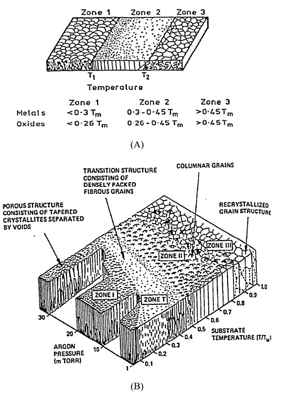
| [105] | Movchan B, Demchishin A (1969) Structure and properties of thick condensates of nickel, titanium, tungsten, aluminum oxides, and zirconium dioxide in vacuum. Fiz Metal Metalloved 28: 653–660. |
| [106] |
Thornton JA (1977) High rate thick film growth. Annu Rev Mater Sci 7: 239–260. doi: 10.1146/annurev.ms.07.080177.001323
|
| [107] |
Messier R, Giri A, Roy R (1984) Revised structure zone model for thin film physical structure. J Vac Sci Technol A 2: 500–503. doi: 10.1116/1.572604
|
| [108] | Singh V (2004) Synthesis, structure, and tribological behavior of nanocomposite DLC based thin films [PhD thesis]. Louisiana State University. |
| [109] | Dresden-rossendorf I, Doctor G (2010) Growth, structure and magnetic properties of magnetron sputtered FePt thin films [PhD thesis]. Technische Universität Dresden. |
| [110] |
Wang B, Fu X, Song S, et al. (2018) Simulation and Optimization of Film Thickness Uniformity in Physical Vapor Deposition. Coatings 8: 325. doi: 10.3390/coatings8090325
|
| [111] |
Divi S, Chatterjee A (2014) Study of Silicon Thin Film Growth at High Deposition Rates Using Parallel Replica Molecular Dynamics Simulations. Energy Procedia 54: 270–280. doi: 10.1016/j.egypro.2014.07.270
|
| [112] | Allen MP (2004) Introduction to molecular dynamics simulation, In: Attig N, Binder K, Grubmuller H, Computational soft matter: from synthetic polymers to proteins, 23: 1–28. |
| [113] | Sutmann G (2002) Classical molecular dynamics and parallel computing, Germany: FZJ-ZAM-IB. |
| [114] | Rasoulian S, Ricardez-Sandoval LA (2015) Worst-case and distributional robustness analysis of a thin film deposition process. 9th International Symposium on Advanced Control of Chemical Processes, 7–10. |
| [115] |
Li J, Croiset E, Ricardez-Sandoval L (2015) Carbon nanotube growth: First-principles-based kinetic Monte Carlo model. J Catal 326: 15–25. doi: 10.1016/j.jcat.2015.03.010
|
| [116] |
Family F (1986) Scaling of rough surfaces: effects of surface diffusion. J Phys A 19: 441. doi: 10.1088/0305-4470/19/8/006
|
| [117] |
Tang L, Nattermann T (1991) Kinetic roughening in molecular-beam epitaxy. Phys Rev Lett 66: 2899. doi: 10.1103/PhysRevLett.66.2899
|
| [118] |
Bhute VJ, Chatterjee A (2013) Building a kinetic Monte Carlo model with a chosen accuracy. J Chem Phys 138: 244112. doi: 10.1063/1.4812319
|
| [119] |
Bhute VJ, Chatterjee A (2013) Accuracy of a Markov state model generated by searching for basin escape pathways. J Chem Phys 138: 084103. doi: 10.1063/1.4792439
|
| [120] |
Lou Y, Christofides PD (2003) Estimation and control of surface roughness in thin film growth using kinetic Monte-Carlo models. Chem Eng Sci 58: 3115–3129. doi: 10.1016/S0009-2509(03)00166-0
|
| [121] |
Theodoropoulou A, Adomaitis RA, Zafiriou E (1998) Model reduction for optimization of rapid thermal chemical vapor deposition systems. IEEE T Semiconduct M 11: 85–98. doi: 10.1109/66.661288
|
| [122] |
Middlebrooks SA, Rawlings JB (2007) Model Predictive Control of Si1−xGex Thin Film Chemical–Vapor Deposition. IEEE T Semiconduct M 20: 114–125. doi: 10.1109/TSM.2007.895203
|
| [123] |
Rasoulian S, Ricardez-Sandoval LA (2015) Robust multivariable estimation and control in an epitaxial thin film growth process under uncertainty. J Process Contr 34: 70–81. doi: 10.1016/j.jprocont.2015.07.002
|
| [124] |
Ricardez‐Sandoval LA (2011) Current challenges in the design and control of multiscale systems. Can J Chem Eng 89: 1324–1341. doi: 10.1002/cjce.20607
|
| [125] |
Vlachos DG (2005) A review of multiscale analysis: examples from systems biology, materials engineering, and other fluid–surface interacting systems. Adv Chem Eng 30: 1–61. doi: 10.1016/S0065-2377(05)30001-9
|
| [126] |
Chaffart D, Ricardez-Sandoval LA (2018) Optimization and control of a thin film growth process: A hybrid first principles/artificial neural network based multiscale modelling approach. Comput Chem Eng 119: 465–479. doi: 10.1016/j.compchemeng.2018.08.029
|
| [127] |
Jensen KF, Rodgers ST, Venkataramani R (1998) Multiscale modeling of thin film growth. Curr Opin Solid St M 3: 562–569. doi: 10.1016/S1359-0286(98)80026-0
|
| [128] |
Baumann F, Chopp D, De La Rubia TD, et al. (2001) Multiscale modeling of thin-film deposition: applications to Si device processing. MRS Bull 26: 182–189. doi: 10.1557/mrs2001.40
|
| [129] |
Zhang P, Zheng X, Wu S, et al. (2004) Kinetic Monte Carlo simulation of Cu thin film growth. Vacuum 72: 405–410. doi: 10.1016/j.vacuum.2003.08.013
|
| [130] |
Evans RD, Ricardez-Sandoval LA (2014) Multi-scenario modelling of uncertainty in stochastic chemical systems. J Comput Phys 273: 374–392. doi: 10.1016/j.jcp.2014.05.028
|
| [131] |
Chaffart D, Ricardez-Sandoval LA (2017) Robust dynamic optimization in heterogeneous multiscale catalytic flow reactors using polynomial chaos expansion. J Process Contr 60: 128–140. doi: 10.1016/j.jprocont.2017.07.002
|
| [132] |
Rasoulian S, Ricardez-Sandoval LA (2016) Stochastic nonlinear model predictive control applied to a thin film deposition process under uncertainty. Chem Eng Sci 140: 90–103. doi: 10.1016/j.ces.2015.10.004
|
| [133] |
Rasoulian S, Ricardez-Sandoval LA (2015) A robust nonlinear model predictive controller for a multiscale thin film deposition process. Chem Eng Sci 136: 38–49. doi: 10.1016/j.ces.2015.02.002
|
| [134] | Allgöwer F, Findeisen R, Nagy ZK (2004) Nonlinear model predictive control: From theory to application. J Chin Inst Chem Engrs 35: 299–315. |
| [135] |
Hu G, Orkoulas G, Christofides PD (2009) Modeling and control of film porosity in thin film deposition. Chem Eng Sci 64: 3668–3682. doi: 10.1016/j.ces.2009.05.008
|
| [136] |
Li C, Song S, Gibson D, et al. (2017) Modeling and validation of uniform large-area optical coating deposition on a rotating drum using microwave plasma reactive sputtering. Appl Optics 56: C65–C70. doi: 10.1364/AO.56.000C65
|
| [137] |
Heirung TAN, Paulson JA, O'Leary J, et al. (2018) Stochastic model predictive control-how does it work? Comput Chem Eng 114: 158–170. doi: 10.1016/j.compchemeng.2017.10.026
|
| [138] | Koronaki E, Gkinis P, Beex L, et al. (2018) Classification of states and model order reduction of large scale Chemical Vapor Deposition processes with solution multiplicity. Comput Chem Eng 121: 148–157. |
| [139] |
Divi S, Chatterjee A (2014) Study of Silicon Thin Film Growth at High Deposition Rates Using Parallel Replica Molecular Dynamics Simulations. Energy Procedia 54: 270–280. doi: 10.1016/j.egypro.2014.07.270
|
Figures(4)

Olayinka Oluwatosin Abegunde, Esther Titilayo Akinlabi, Oluseyi Philip Oladijo, Stephen Akinlabi, Albert Uchenna Ude. Overview of thin film deposition techniques[J]. AIMS Materials Science, 2019, 6(2): 174-199. doi: 10.3934/matersci.2019.2.174


 DownLoad: