Citation: Clemens Liewald, Simon Noever, Stefan Fischer, Janina Roemer, Tobias U. Schülli, Bert Nickel. Microdiffraction imaging—a suitable tool to characterize organic electronic devices[J]. AIMS Materials Science, 2015, 2(4): 369-378. doi: 10.3934/matersci.2015.4.369

| [1] |
Bredas JL, Beljonne D, Coropceanu V, et al. (2004) Charge-transfer and energy-transfer processes in pi-conjugated oligomers and polymers: A molecular picture. Chem Rev 104: 4971-5003. doi: 10.1021/cr040084k

|
| [2] |
He T, Stolte M, Burschka C, et al. (2015) Single-crystal field-effect transistors of new Cl2-NDI polymorph processed by sublimation in air. Nat Commun 6: 5954. doi: 10.1038/ncomms6954
|
| [3] |
Tang Q, Zhang DQ, Wang SL, et al. (2009) A Meaningful Analogue of Pentacene: Charge Transport, Polymorphs, and Electronic Structures of Dihydrodiazapentacene. Chem Mater 21: 1400-1405. doi: 10.1021/cm9001916
|
| [4] |
Schiefer S, Huth M, Dobrinevski A, et al. (2007) Determination of the crystal structure of substrate-induced pentacene polymorphs in fiber structured thin films. J Am Chem Soc 129: 10316-10317. doi: 10.1021/ja0730516
|
| [5] |
Mattheus CC, Dros AB, Baas J, et al. (2003) Identification of polymorphs of pentacene. Synth Met 138: 475-481. doi: 10.1016/S0379-6779(02)00467-8
|
| [6] |
Westermeier C, Cernescu A, Amarie S, et al. (2014) Sub-micron phase coexistence in small-molecule organic thin films revealed by infrared nano-imaging. Nat Commun 5: 5101. doi: 10.1038/ncomms6101
|
| [7] |
Durr AC, Schreiber F, Kelsch M, et al. (2002) Morphology and thermal stability of metal contacts on crystalline organic thin films. Adv Mater 14: 961-963. doi: 10.1002/1521-4095(20020705)14:13/14<961::AID-ADMA961>3.0.CO;2-X
|
| [8] |
Kahn A, Koch N, Gao WY (2003) Electronic structure and electrical properties of interfaces between metals and pi-conjugated molecular films. J Polym Sci Part B Polym Phys 41: 2529-2548. doi: 10.1002/polb.10642
|
| [9] |
Necliudov PV, Shur MS, Gundlach DJ, et al. (2003) Contact resistance extraction in pentacene thin film transistors. Solid State Electron 47: 259-262. doi: 10.1016/S0038-1101(02)00204-6
|
| [10] | Klauk H, (2006) Organic Electronics: Materials, Manufacturing, and Applications, 1 Eds., Wiley-VCH. |
| [11] | Dam HF, Andersen TR, Pedersen EBL, et al. (2015) Enabling flexible polymer tandem solar cells by 3D ptychographic imaging. Adv Energy Mater 5: 1400736. |
| [12] |
Fuller T, Banhart F (1996) In situ observation of the formation and stability of single fullerene molecules under electron irradiation. Chem Phys Lett 254: 372-378. doi: 10.1016/0009-2614(96)00338-7
|
| [13] | Tolan M, (2013) X-Ray Scattering from Soft-Matter Thin Films: Materials Science and Basic Research, Springer. |
| [14] |
Fritz SE, Martin SM, Frisbie CD, et al. (2004) Structural characterization of a pentacene monolayer on an amorphous SiO2 substrate with grazing incidence X-ray diffraction. J Am Chem Soc 126: 4084-4085. doi: 10.1021/ja049726b
|
| [15] |
Noever SJ, Fischer S, Nickel B (2013) Dual Channel Operation Upon n-Channel Percolation in a Pentacene-C60 Ambipolar Organic Thin Film Transistor. Adv Mater 25: 2147-2151. doi: 10.1002/adma.201203964
|
| [16] |
Qazilbash MM, Tripathi A, Schafgans AA, et al. (2011) Nanoscale imaging of the electronic and structural transitions in vanadium dioxide. Phys Rev B 83: 165108. doi: 10.1103/PhysRevB.83.165108
|
| [17] |
Chahine GA, Richard MI, Homs-Regojo RA, et al. (2014) Imaging of strain and lattice orientation by quick scanning X-ray microscopy combined with three-dimensional reciprocal space mapping. J Appl Crystallogr 47: 762-769. doi: 10.1107/S1600576714004506
|
| [18] |
Chahine GA, Zoellner MH, Richard M-I, et al. (2015) Strain and lattice orientation distribution in SiN/Ge complementary metal-oxide-semiconductor compatible light emitting microstructures by quick x-ray nano-diffraction microscopy. Appl Phys Lett 106: 071902. doi: 10.1063/1.4909529
|
| [19] |
Zoellner MH, Richard M-I, Chahine GA, et al. (2015) Imaging Structure and Composition Homogeneity of 300 mm SiGe Virtual Substrates for Advanced CMOS Applications by Scanning X-ray Diffraction Microscopy. ACS Appl Mater Interfaces 7: 9031-9037. doi: 10.1021/am508968b
|
| [20] |
Paci B, Bailo D, Albertini VR, et al. (2013) Spatially-resolved in-situ structural study of organic electronic devices with nanoscale resolution: the plasmonic photovoltaic case study. Adv Mater 25: 4760-4765. doi: 10.1002/adma.201301682
|
| [21] | Reich C, Hochrein MB, Krause B, et al. (2005) A microfluidic setup for studies of solid-liquid interfaces using x-ray reflectivity and fluorescence microscopy. Rev Sci Instrum 76. |
| [22] |
Dimitrakopoulos CD, Brown AR, Pomp A (1996) Molecular beam deposited thin films of pentacene for organic field effect transistor applications. J Appl Phys 80: 2501-2508. doi: 10.1063/1.363032
|
| [23] |
Knipp D, Street RA, Volkel A, et al. (2003) Pentacene thin film transistors on inorganic dielectrics: Morphology, structural properties, and electronic transport. J Appl Phys 93: 347-355. doi: 10.1063/1.1525068
|
| [24] | Yanagisawa H, Tamaki T, Nakamura M, et al. (2004) Structural and electrical characterization of pentacene films on SiO2 grown by molecular beam deposition. Thin Solid Films 464: 398-402. |
| [25] |
Seeck OH, Deiter C, Pflaum K, et al. (2012) The high-resolution diffraction beamline P08 at PETRA III. J Synchrotron Radiat 19: 30-38. doi: 10.1107/S0909049511047236
|
| [26] | Ponchut C, Rigal JM, Clément J, et al. (2011) MAXIPIX, a fast readout photon-counting X-ray area detector for synchrotron applications. J Instrum 6: C01069. |
| [27] | Kaefer D, Ruppel L, Witte G (2007) Growth of pentacene on clean and modified gold surfaces. Phys Rev B 75. |
| [28] |
Bouchoms IPM, Schoonveld WA, Vrijmoeth J, et al. (1999) Morphology identification of the thin film phases of vacuum evaporated pentacene on SiO2 substrates. Synth Met 104: 175-178. doi: 10.1016/S0379-6779(99)00050-8
|
| [29] |
Govyadinov AA, Mastel S, Golmar F, et al. (2014) Recovery of Permittivity and Depth from Near-Field Data as a Step toward Infrared Nanotomography. ACS Nano 8: 6911-6921. doi: 10.1021/nn5016314
|
| [30] |
Seiki N, Shoji Y, Kajitani T, et al. (2015) Rational synthesis of organic thin films with exceptional long-range structural integrity. Science 348: 1122-1126. doi: 10.1126/science.aab1391
|
| [31] |
Collins BA, Cochran JE, Yan H, et al. (2012) Polarized X-ray scattering reveals non-crystalline orientational ordering in organic films. Nat Mater 11: 536-543. doi: 10.1038/nmat3310
|
| [32] |
Hub C, Burkhardt M, Halik M, et al. (2010) In situ STXM investigations of pentacene-based OFETs during operation. J Mater Chem 20: 4884-4887. doi: 10.1039/c0jm00423e
|
| [33] |
Weickert J, Dunbar RB, Hesse HC, et al. (2011) Nanostructured Organic and Hybrid Solar Cells. Adv Mater 23: 1810-1828. doi: 10.1002/adma.201003991
|
| [34] |
Westermeier C, Fiebig M, Nickel B (2013) Mapping of trap densities and hotspots in pentacene thin-film transistors by frequency-resolved scanning photoresponse microscopy. Adv Mater 25: 5719-5724. doi: 10.1002/adma.201300958
|
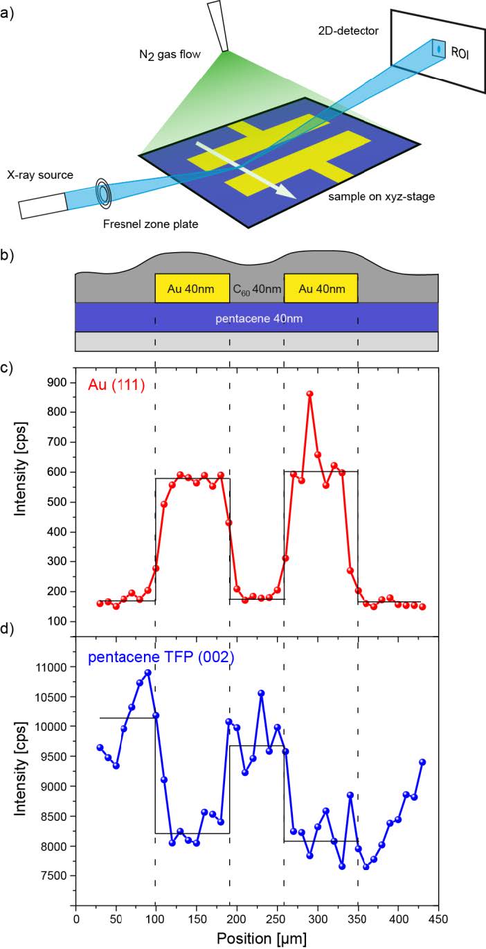
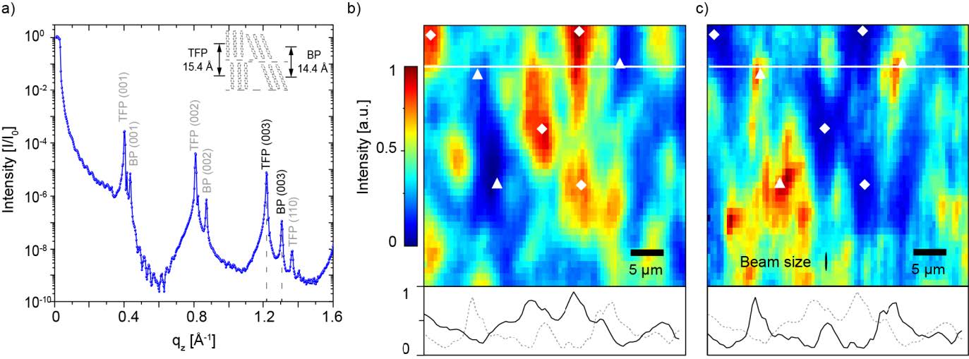
Figures(2)

Clemens Liewald, Simon Noever, Stefan Fischer, Janina Roemer, Tobias U. Schülli, Bert Nickel. Microdiffraction imaging—a suitable tool to characterize organic electronic devices[J]. AIMS Materials Science, 2015, 2(4): 369-378. doi: 10.3934/matersci.2015.4.369


 DownLoad: