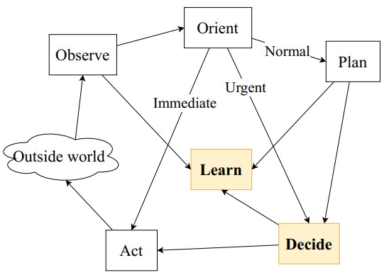
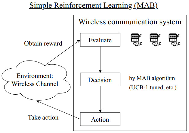
Data-driven and feedback cycle-based approaches are necessary to optimize the performance of modern complex wireless communication systems. Machine learning technologies can provide solutions for these requirements. This study shows a comprehensive framework of optimizing wireless communication systems and proposes two optimal decision schemes that have not been well-investigated in existing research. The first one is supervised learning modeling and optimal decision making by optimization, and the second is a simple and implementable reinforcement learning algorithm. The proposed schemes were verified through real-world experiments and computer simulations, which revealed the necessity and validity of this research.
Citation: Koji Oshima, Daisuke Yamamoto, Atsuhiro Yumoto, Song-Ju Kim, Yusuke Ito, Mikio Hasegawa. Online machine learning algorithms to optimize performances of complex wireless communication systems[J]. Mathematical Biosciences and Engineering, 2022, 19(2): 2056-2094. doi: 10.3934/mbe.2022097
Data-driven and feedback cycle-based approaches are necessary to optimize the performance of modern complex wireless communication systems. Machine learning technologies can provide solutions for these requirements. This study shows a comprehensive framework of optimizing wireless communication systems and proposes two optimal decision schemes that have not been well-investigated in existing research. The first one is supervised learning modeling and optimal decision making by optimization, and the second is a simple and implementable reinforcement learning algorithm. The proposed schemes were verified through real-world experiments and computer simulations, which revealed the necessity and validity of this research.

| [1] |
Y. LeCun, Y. Bengio, G. Hinton, Deep learning, Nature, 521 (2015), 436–444. doi: 10.1038/nature14539. doi: 10.1038/nature14539

|
| [2] | Google AI Blog, AlphaGo: Mastering the ancient game of Go with Machine Learning, 2016. Available from: https://ai.googleblog.com/2016/01/alphago-mastering-ancient-game-of-go.html. |
| [3] | The 3rd Generation Partnership Project (3GPP). Available from: https://www.3gpp.org/specifications/specifications. |
| [4] |
H. Yang, A. Alphones, Z. Xiong, D. Niyato, J. Zhao, K. Wu, Artificial-intelligence-enabled intelligent 6G networks, IEEE Network, 34 (2020), 272–280. doi: 10.1109/MNET.011.2000195. doi: 10.1109/MNET.011.2000195
|
| [5] |
A. Goldsmith, S. Chua, Adaptive coded modulation for fading channels, IEEE Trans. Commun., 46 (1998), 595–602. doi: 10.1109/26.668727. doi: 10.1109/26.668727
|
| [6] |
D. Gesbert, S. Kiani, A. Gjendemsjo, G. Oien, Adaptation, coordination, and distributed resource allocation in interference-limited wireless networks, Proc. IEEE, 95 (2007), 2393–2409. doi: 10.1109/JPROC.2007.907125. doi: 10.1109/JPROC.2007.907125
|
| [7] |
J. Lu, T. T. Tjhung, F. Adachi, C. L. Huang, BER performance of OFDM-MDPSK system in frequency-selective Rician fading with diversity reception, IEEE Trans. Veh. Technol., 49 (2000), 1216–1225. doi: 10.1109/25.875231. doi: 10.1109/25.875231
|
| [8] |
S. T. Chung, A. J. Goldsmith, Degrees of freedom in adaptive modulation: a unified view, IEEE Trans. Commun., 49 (2001), 1561–1571. doi: 10.1109/VETECS.2001.944588. doi: 10.1109/VETECS.2001.944588
|
| [9] |
D. Qiao, S. Choi, K. G. Shin, Goodput analysis and link adaptation for IEEE 802.11a wireless LANs, IEEE Trans. Mobile Comput., 1 (2002), 278–291. doi: 10.1109/TMC.2002.1175541 doi: 10.1109/TMC.2002.1175541
|
| [10] |
E. Peh, Y. Liang, Y. Guan, Y. Zeng, Optimization of cooperative sensing in cognitive radio networks: A sensing-throughput tradeoff view, IEEE Trans. Veh. Technol., 58 (2009), 5294–5299. doi: 10.1109/TVT.2009.2028030. doi: 10.1109/TVT.2009.2028030
|
| [11] |
G. Bianchi, Performance analysis of the IEEE 802.11 distributed coordination function, IEEE J. Sel. Areas Commun., 18 (2000), 535–547. doi: 10.1109/49.840210. doi: 10.1109/49.840210
|
| [12] |
J. Mitola, G. Q. Maguire, Cognitive radio: making software radios more personal, IEEE Pers. Commun., 6 (1999), 13–18. doi: 10.1109/98.788210. doi: 10.1109/98.788210
|
| [13] |
S. Haykin, Cognitive radio: Brain-empowered wireless communications, IEEE J. Sel. Areas Commun., 23 (2005), 201–220. doi: 10.1109/JSAC.2004.839380. doi: 10.1109/JSAC.2004.839380
|
| [14] |
M. G. Kibria, K. Nguyen, G. P. Villardi, O. Zhao, K. Ishizu, F. Kojima, Big data analytics, machine learning, and artificial intelligence in next-generation wireless networks, IEEE Access, 6 (2018), 32328–32338. doi: 10.1109/ACCESS.2018.2837692. doi: 10.1109/ACCESS.2018.2837692
|
| [15] |
M. Chen, U. Challita, W. Saad, C. Yin, M. Debbah, Artificial neural networks-based machine learning for wireless networks: A tutorial, IEEE Commun. Surv. Tutor., 21 (2019), 3039–3071. doi: 10.1109/COMST.2019.2926625. doi: 10.1109/COMST.2019.2926625
|
| [16] |
J. Wang, C. Jiang, H. Zhang, Y. Ren, K. -C. Chen, L. Hanzo, Thirty years of machine learning: The road to Pareto-optimal wireless networks, IEEE Commun. Surv. Tutor., 22 (2020), 1472–1514. doi: 10.1109/COMST.2020.2965856. doi: 10.1109/COMST.2020.2965856
|
| [17] |
M. Kulin, T. Kazaz, I. Moerman, E. De Poorter, End-to-end learning from spectrum data: A deep learning approach for wireless signal identification in spectrum monitoring applications, IEEE Access, 6 (2018), 18484–18501. doi: 10.1109/ACCESS.2018.2818794. doi: 10.1109/ACCESS.2018.2818794
|
| [18] |
C. Jiang, H. Zhang, Y. Ren, Z. Han, K. Chen, L. Hanzo, Machine learning paradigms for next-generation wireless networks, IEEE Wireless Commun., 24 (2017), 98–105. doi: 10.1109/MWC.2016.1500356WC. doi: 10.1109/MWC.2016.1500356WC
|
| [19] |
R. Li, Z. Zhao, X. Zhou, G. Ding, Y. Chen, Z. Wang, et al., Intelligent 5G: When cellular networks meet artificial intelligence, IEEE Wireless Commun., 24 (2017), 175–183. doi: 10.1109/MWC.2017.1600304WC. doi: 10.1109/MWC.2017.1600304WC
|
| [20] | T. M. Cover, J. A. Thomas, Elements of Information Theory, Wiley, 1991. |
| [21] |
Z. M. Fadlullah, F. Tang, B. Mao, N. Kato, O. Akashi, T. Inoue, et al., State-of-the-art deep learning: Evolving machine intelligence toward tomorrow's intelligent network traffic control systems, IEEE Commun. Surv. Tutor., 19 (2017), 2432–2455. doi: 10.1109/COMST.2017.2707140. doi: 10.1109/COMST.2017.2707140
|
| [22] |
H. Ye, G. Y. Li, B. Juang, Power of deep learning for channel estimation and signal detection in OFDM systems, IEEE Wireless Commun. Lett., 7 (2018), 114–117. doi: 10.1109/LWC.2017.2757490. doi: 10.1109/LWC.2017.2757490
|
| [23] |
H. Huang, J. Yang, H. Huang, Y. Song, G. Gui, Deep learning for super-resolution channel estimation and DOA estimation based massive MIMO system, IEEE Trans. Veh. Technol., 67 (2018), 8549–8560. doi: 10.1109/TVT.2018.2851783. doi: 10.1109/TVT.2018.2851783
|
| [24] |
R. W. Ouyang, A. K. Wong, C. Lea, M. Chiang, Indoor location estimation with reduced calibration exploiting unlabeled data via hybrid generative/discriminative learning, IEEE Trans. Mob. Comput., 11 (2012), 1613–1626. doi: 10.1109/TMC.2011.193. doi: 10.1109/TMC.2011.193
|
| [25] |
Y. Chen, Q. Yang, J. Yin, X. Chai, Power-efficient access-point selection for indoor location estimation, IEEE Trans. Knowl. Data. Eng., 18 (2006), 877–888. doi: 10.1109/TKDE.2006.112. doi: 10.1109/TKDE.2006.112
|
| [26] |
S. Marano, W. M. Gifford, H. Wymeersch, M. Z. Win, NLOS identification and mitigation for localization based on UWB experimental data, IEEE J. Sel. Areas Commun., 28 (2010), 1026–1035. doi: 10.1109/JSAC.2010.100907. doi: 10.1109/JSAC.2010.100907
|
| [27] |
B. Mager, P. Lundrigan, N. Patwari, Fingerprint-based device-free localization performance in changing environments, IEEE J. Sel. Areas Commun., 33 (2015), 2429–2438. doi: 10.1109/JSAC.2015.2430515. doi: 10.1109/JSAC.2015.2430515
|
| [28] |
L. U. Khan, I. Yaqoob, M. Imran, Z. Han, C. S. Hong, 6G wireless systems: A vision, architectural elements, and future directions, IEEE Access, 8 (2020), 147029–147044. doi: 10.1109/ACCESS.2020.3015289. doi: 10.1109/ACCESS.2020.3015289
|
| [29] |
Y. He, C. Liang, F. R. Yu, Z. Han, Trust-based social networks with computing, caching and communications: A deep reinforcement learning approach, IEEE Trans. Network Sci. Eng., 7 (2020), 66–79. doi: 10.1109/TNSE.2018.2865183. doi: 10.1109/TNSE.2018.2865183
|
| [30] |
L. Li, Y. Xu, J. Yin, W. Liang, X. Li, W. Chen, Z. Han, Deep reinforcement learning approaches for content caching in cache-enabled D2D networks, IEEE Internet Things J., 7 (2020), 544–557. doi: 10.1109/JIOT.2019.2951509. doi: 10.1109/JIOT.2019.2951509
|
| [31] |
F. B. Mismar, B. L. Evans, A. Alkhateeb, Deep reinforcement learning for 5G networks: Joint beamforming, power control, and interference coordination, IEEE Trans. Commun., 68 (2020), 1581–1592. doi: 10.1109/TCOMM.2019.2961332. doi: 10.1109/TCOMM.2019.2961332
|
| [32] |
X. Fu, F. R. Yu, J. Wang, Q. Qi, J. Liao, Dynamic service function chain embedding for NFV-enabled IoT: A deep reinforcement learning approach, IEEE Trans. Wireless Commun., 19 (2020), 507–519. doi: 10.1109/TWC.2019.2946797. doi: 10.1109/TWC.2019.2946797
|
| [33] |
H. Huang, Y. Yang, H. Wang, Z. Ding, H. Sari, F. Adachi, Deep reinforcement learning for UAV navigation through massive MIMO technique, IEEE trans. Veh. Technol., 69 (2020), 1117–1121. doi: 10.1109/TVT.2019.2952549. doi: 10.1109/TVT.2019.2952549
|
| [34] |
Z. Zhang, H. Chen, M. Hua, C. Li, Y. Huang, L. Yang, Double coded caching in ultra dense networks: Caching and multicast scheduling via deep reinforcement learning, IEEE Trans. Commun., 68 (2020), 1071–1086. doi: 10.1109/TCOMM.2019.2955490. doi: 10.1109/TCOMM.2019.2955490
|
| [35] | H. Robbins, Some aspects of the sequential design of experiments, Bull. Amer. Math. Soc., 58 (1952), 527–535. |
| [36] | L. Lai, H. E. Jiang, H. V. Poor, Medium access in cognitive radio networks: A competitive multi-armed bandit frame work, in Processing of IEEE 42th Asilomar Conference on Signals, System, and Computer (2008), 98–102. doi: 10.1109/ACSSC.2008.5074370. |
| [37] |
L. Lai, H. E. Jiang, H. V. Poor, Cognitive medium access: Exploration, exploitation, and competition, IEEE Trans. Mobile Comput., 10 (2011), 239–253. doi: 10.1109/TMC.2010.65. doi: 10.1109/TMC.2010.65
|
| [38] |
S. Maghsudi, E. Hossain, Multi-armed bandits with application to 5G small cells, IEEE Wireless Commun., 23 (2016), 64–73. doi: 10.1109/MWC.2016.7498076. doi: 10.1109/MWC.2016.7498076
|
| [39] |
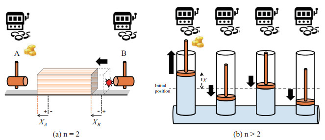
S. J. Kim, M. Aono, M. Hara, Tug-of-war model for the two-bandit problem: Nonlocally-correlated parallel exploration via resource conservation, Biosystems, 101 (2010), 29–36. doi: 10.1016/j.biosystems.2010.04.002. doi: 10.1016/j.biosystems.2010.04.002
|
| [40] |
Z. Zhao, E. Schiller, E. Kalogeiton, T. Braun, B. Stiller, M. T. Garip, et al., Autonomic communications in software-driven networks, IEEE J. Sel. Areas Commun., 35 (2017), 2431–2445. doi: 10.1109/JSAC.2017.2760354. doi: 10.1109/JSAC.2017.2760354
|
| [41] | Radio Spectrum Policy Group, Report on Collective Use of Spectrum and Other Sharing Approaches, 2011. Available from: https://rspg-spectrum.eu/wp-content/uploads/2013/05/rspg11_392_report_CUS_other_approaches_final.pdf. |
| [42] | CEPT Electronic Communications Committee, ECC Report 205–Licensed Shared Access (LSA), 2014. Available from: http://spectrum.welter.fr/international/cept/ecc-reports/ecc-report-205-LSA-2300-MHz-2400-MHz.pdf. |
| [43] | Reconfigurable Radio Systems (RRS), Information Elements and Protocols for the Interface between the LSA Controller (LC) and LSA Repository (LR) for the Operation of Licensed Shared Access (LSA) in the 2300 MHz–2400 MHz Band, 2017. Available from: https://www.etsi.org/deliver/etsi_ts/103300_103399/103379/01.01.01_60/ts_103379v010101p.pdf |
| [44] |
S. Haykin, P. Setoodeh, S. Feng, D. Findlay, Cognitive dynamic system as the brain of complex networks, IEEE J. Sel. Areas Commun., 34 (2016), 2791–2800. doi: 10.1109/JSAC.2016.2605240. doi: 10.1109/JSAC.2016.2605240
|
| [45] |
M. Hasegawa, H. Hirai, K. Nagano, H. Harada, K. Aihara, Optimization for centralized and decentralized cognitive radio networks, Proc. IEEE, 102 (2014), 574–584. doi: 10.1109/JPROC.2014.2306255. doi: 10.1109/JPROC.2014.2306255
|
| [46] |
Y. Kon, K. Hashiguchi, M. Ito, M. Hasegawa, K. Ishizu, H. Murakami, et al., Autonomous throughput improvement scheme using machine learning algorithms for heterogeneous wireless networks aggregation, IEICE Trans. Commun., 95 (2012), 1143–1151. doi: 10.1587/transcom.E95.B.1143. doi: 10.1587/transcom.E95.B.1143
|
| [47] | IEEE, IEEE Standard for Architectural Building Blocks Enabling Network-Device Distributed Decision Making for Optimized Radio Resource Usage in Heterogeneous Wireless Access Networks, 2009. Available from: https://ieeexplore.ieee.org/document/4798288. |
| [48] |
R. Combes, A. Proutiere, Dynamic rate and channel selection in cognitive radio systems, IEEE J. Sel. Areas Commun., 33 (2015), 910–921. doi: 10.1109/JSAC.2014.2361084. doi: 10.1109/JSAC.2014.2361084
|
| [49] |
D. Shiung, Y. Yang, Rate enhancement for cognitive radios using the relationship between transmission rate and signal-to-interference ratio statistics, IET Commun., 7 (2013). doi: 10.1049/iet-com.2013.0047. doi: 10.1049/iet-com.2013.0047
|
| [50] |
J. Lehtomaki, M. Benitez, K. Umebayashi, M. Juntti, Improved channel occupancy rate estimation, IEEE Trans. Commun., 63 (2015), 643–654. doi: 10.1109/TCOMM.2015.2402195. doi: 10.1109/TCOMM.2015.2402195
|
| [51] | B. E. Boser, I. M. Guyon, V. N. Vapnik, A training algorithm for optimal margin classifiers, in Proceedings of the fifth annual workshop on Computational learning theory, (1992), 144–152. doi: 10.1145/130385.130401. |
| [52] | V. Vapnik, S. Golowich, A. Smola, Support vector method for function approximation, regression estimation, and signal processing, Adv. Neural Inf. Process. Syst., 1997 (1997), 281–287. |
| [53] |
K. Oshima, T. Kobayashi, Y. Taenaka, K. Kuroda, M. Hasegawa, Wireless network optimization method based on cognitive cycle using machine learning, IEICE Commun. Express, 7 (2018), 278–283. doi: 10.1587/comex.2018XBL0061. doi: 10.1587/comex.2018XBL0061
|
| [54] | K. Oshima, T. Kobayashi, Y. Taenaka, K. Kuroda, M. Hasegawa, Autonomous wireless system optimization method based on cross-layer modeling using machine learning, in IEEE International Conference on Ubiquitous and Future Networks, (2019), 239–244. doi: 10.1109/ICUFN.2019.8806031. |
| [55] | J. Kennedy, R. Eberhart, Particle swarm optimization, in Proceedings of ICNN'95-International Conference on Neural Networks, 4 (1995), 1942–1948. doi: 10.1109/ICNN.1995.488968. |
| [56] |
V. Kadirkamanathan, K. Selvarajah, P. J. Fleming, Stability analysis of the particle dynamics in particle swarm optimizer, IEEE Trans. Evol. Comput., 10 (2006), 245–255. doi: 10.1109/TEVC.2005.857077. doi: 10.1109/TEVC.2005.857077
|
| [57] | Scalable Network Technologies, Inc., Available from: https://www.scalable-networks.com. |
| [58] | Beyond 5G/6G White Paper, National Institute of Information and Communications Technology, 2021. Available from: https://beyond5g.nict.go.jp/en/download/index.html. |
| [59] |
P. V. R. Ferreira, R. Paffenroth, A. M. Wyglinski, T. M. Hackett, S. G. Bilen, R. C. Reinhart, et al., Multiobjective reinforcement learning for cognitive satellite communications using deep neural network ensembles, IEEE J. Sel. Areas Commun., 36 (2018). doi: 10.1109/JSAC.2018.2832820. doi: 10.1109/JSAC.2018.2832820
|
| [60] | N. Cardwell, Y. Cheng, C. S. Gunn, S. H. Yeganeh, V. Jacobson, BBR: congestion-based congestion control, ACM Queue, 14 (2016), 20–53. |
| [61] |
H. Yang, Z. Xiong, J. Zhao, D. Niyato, Q. Wu, L. Xiao, Deep reinforcement learning-based intelligent reflecting surface for secure wireless communications, IEEE Trans. Wireless Commun., 20 (2021), 375–388. doi: 10.1109/TWC.2020.3024860. doi: 10.1109/TWC.2020.3024860
|
| [62] |
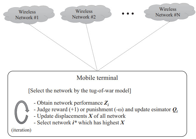
K. Oshima, T. Onishi, S. J. Kim, J. Ma, M. Hasegawa, Efficient wireless network selection by using multi-armed bandit algorithm for mobile terminals, Nonlinear Theory Its Appl. IEICE, 11 (2020), 68–77. doi: 10.1587/nolta.11.68. doi: 10.1587/nolta.11.68
|
| [63] | R. Sutton, A. Barto, Reinforcement Learning: An Introduction, The MIT Press, 1998. |
| [64] |
N. D. Daw, J. P. O'doherty, P. Dayan, B. Seymour, R. J. Dolan, Cortical substrates for exploratory decisions in humans, Nature, 441 (2006), 876–879. doi: 10.1038/nature04766. doi: 10.1038/nature04766
|
| [65] |
P. Auer, N. Cesa-Bianchi, P. Fischer, Finite-time analysis of the multiarmed bandit problem, Mach. Learn., 47 (2002), 235–256. doi: 10.1023/A:1013689704352. doi: 10.1023/A:1013689704352
|
| [66] |
S. J. Kim, M. Aono, Amoeba-inspired algorithm for cognitive medium access, NOLTA, 5 (2014), 198–209. doi: 10.1587/nolta.5.198. doi: 10.1587/nolta.5.198
|
| [67] |
S. J. Kim, M. Aono, E. Nameda, Efficient decision-making by volume-conserving physical object, New J. Phys., 17 (2015). doi: 10.1088/1367-2630/17/8/083023. doi: 10.1088/1367-2630/17/8/083023
|
| [68] |
S. J. Kim, M. Aono, E. Nameda, Decision maker based on atomic switches, AIMS Mater. Sci., 3 (2016), 245–259. doi: 10.3934/matersci.2016.1.245. doi: 10.3934/matersci.2016.1.245
|
| [69] |
J. Ma, S. Hasegawa, S. J. Kim, M. Hasegawa, A reinforcement-learning-based distributed resource selection algorithm for massive IoT, Appl. Sci., 9 (2019). doi: 10.3390/app9183730. doi: 10.3390/app9183730
|
| [70] |
H. Yang, Z. Xiong, J. Zhao, D. Niyato, Q. Wu, H. V. Poor, et al., Intelligent reflecting surface assisted anti-jamming communications: A fast reinforcement learning approach, IEEE Trans. Wireless Commun., 20 (2021), 1963–1974. doi: 10.1109/TWC.2020.3037767. doi: 10.1109/TWC.2020.3037767
|
| [71] |
S. Singh, J. G. Andrews, Joint resource partitioning and offloading in heterogeneous cellular networks, IEEE Trans. Wireless Commun., 13 (2014), 888–901. doi: 10.1109/TWC.2013.120713.130548. doi: 10.1109/TWC.2013.120713.130548
|
| [72] |
C. Liu, M. Li, S. V. Hanly, P. Whiting, Joint downlink user association and interference management in two-tier HetNets with dynamic resource partitioning, IEEE Trans. Veh. Technol., 66 (2017), 1365–1378. doi: 10.1109/TVT.2016.2565538. doi: 10.1109/TVT.2016.2565538
|
| [73] |
V. Sagar, R. Chandramouli, K. P. Subbalakshmi, Software defined access for HetNets, IEEE Commun. Mag., 54 (2016), 84–89. doi: 10.1109/MCOM.2016.7378430. doi: 10.1109/MCOM.2016.7378430
|
| [74] |
A. Keshavarz-Haddad, E. Aryafar, M. Wang, M. Chiang, HetNets selection by clients: Convergence efficiency and practicality, IEEE/ACM Trans. Netw., 25 (2017), 406–419. doi: 10.1109/TNET.2016.2587622. doi: 10.1109/TNET.2016.2587622
|
| [75] | E. Aryafar, A. Keshavarz-Haddad, M. Wang, M. Chiang, RAT selection games in HetNets, in 2013 Proceedings IEEE INFOCOM, (2013), 998–1006. doi: 10.1109/INFCOM.2013.6566889. |
| [76] |
X. Wang, J. Li, L. Wang, C. Yang, Z. Han, Intelligent user-centric network selection: A model-driven reinforcement learning framework, IEEE Access, 7 (2019), 21645–21661. doi: 10.1109/ACCESS.2019.2898205. doi: 10.1109/ACCESS.2019.2898205
|
| [77] |
D. D. Nguyen, H. X. Nguyen, L. B. White, Reinforcement learning with network-assisted feedback for heterogeneous RAT selection, IEEE Trans. Wireless Commun., 19 (2017). doi: 10.1109/TWC.2017.2718526. doi: 10.1109/TWC.2017.2718526
|
| [78] |
K. Kuroda, H. Kato, S. J. Kim, M. Naruse, M. Hasegawa, Improving throughput using multi-armed bandit algorithm for wireless LANs, NOLTA, 9 (2018), 74–81. doi: 10.1587/nolta.9.74. doi: 10.1587/nolta.9.74
|
| [79] | ns-3, ns-3: A Discrete-event Network Simulator for Internet Systems, Available from: https://www.nsnam.org/. |
| [80] |
S. Takeuchi, M. Hasegawa, K. Kanno, A. Uchida, N. Chauvet, M. Naruse, Dynamic channel selection in wireless communications via a multi-armed bandit algorithm using laser chaos time series, Sci. Rep., 10 (2020). doi: 10.1038/s41598-020-58541-2. doi: 10.1038/s41598-020-58541-2
|
| [81] | H. Kanemasa, A. Li, M. Naruse, N. Chauvet, M. Hasegawa, Dynamic channel bonding using laser chaos decision maker in WLANs, 2021 International Conference on Artificial Intelligence in Information and Communication (ICAIIC), (2021), 078–082. doi: 10.1109/ICAIIC51459.2021.9415227. |
| [82] | Z. Duan, N. Okada, A. Li, M. Naruse, N. Chauvet, M. Hasegawa, High-speed optimization of user pairing in NOMA system using laser chaos based MAB algorithm, 2021 International Conference on Artificial Intelligence in Information and Communication (ICAIIC), (2021), 073–077. doi: 10.1109/ICAIIC51459.2021.9415234. |
Figures(21) / Tables(6)

Koji Oshima, Daisuke Yamamoto, Atsuhiro Yumoto, Song-Ju Kim, Yusuke Ito, Mikio Hasegawa. Online machine learning algorithms to optimize performances of complex wireless communication systems[J]. Mathematical Biosciences and Engineering, 2022, 19(2): 2056-2094. doi: 10.3934/mbe.2022097


 DownLoad: