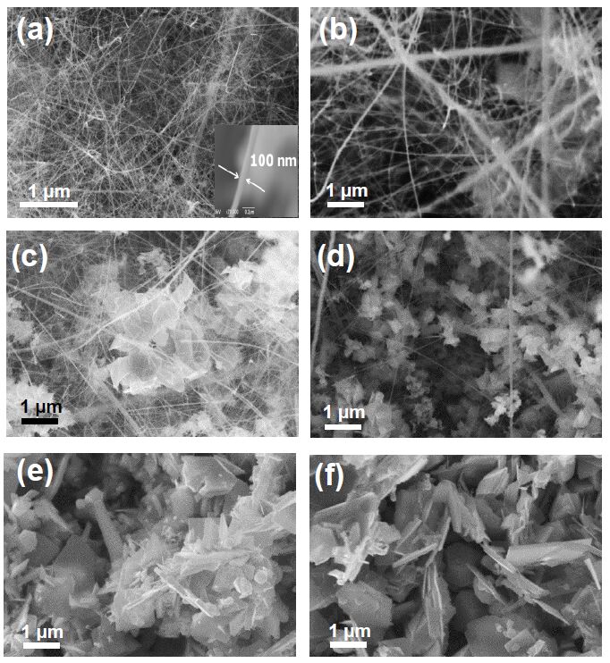
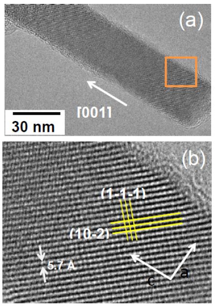
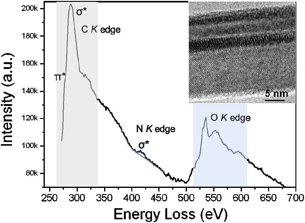
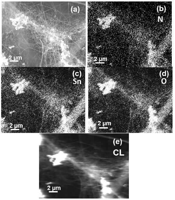
Citation: David Montalvo, Manuel Herrera. Cathodoluminescence of N-doped SnO2 nanowires and microcrystals[J]. AIMS Materials Science, 2016, 3(2): 525-537. doi: 10.3934/matersci.2016.2.525
[1] | Ravipati Praveena, Gottapu. Varaprasada Rao, Karna Balasubrahmanyam, M. Ghanashyam Krishna, Vinjanampati Madhurima . Optical and water repellant properties of Ag/SnO2 bilayer thin films. AIMS Materials Science, 2016, 3(1): 231-244. doi: 10.3934/matersci.2016.1.231 |
[2] | Iñaki López, Teresa Cebriano, Pedro Hidalgo, Emilio Nogales, Javier Piqueras, Bianchi Méndez . The role of impurities in the shape, structure and physical properties of semiconducting oxide nanostructures grown by thermal evaporation. AIMS Materials Science, 2016, 3(2): 425-433. doi: 10.3934/matersci.2016.2.425 |
[3] | Miguel García-Tecedor, Félix del Prado, Carlos Bueno, G. Cristian Vásquez, Javier Bartolomé, David Maestre, Tomás Díaz, Ana Cremades, Javier Piqueras . Tubular micro- and nanostructures of TCO materials grown by a vapor-solid method. AIMS Materials Science, 2016, 3(2): 434-447. doi: 10.3934/matersci.2016.2.434 |
[4] | K. Ravindranadh, K. Durga Venkata Prasad, M.C. Rao . Spectroscopic and luminescent properties of Co2+ doped tin oxide thin films by spray pyrolysis. AIMS Materials Science, 2016, 3(3): 796-807. doi: 10.3934/matersci.2016.3.796 |
[5] | David Jishiashvili, Zeinab Shiolashvili, Archil Chirakadze, Alexander Jishiashvili, Nino Makhatadze, Kakha Gorgadze . Development of low temperature technology for the growth of wide band gap semiconductor nanowires. AIMS Materials Science, 2016, 3(2): 470-485. doi: 10.3934/matersci.2016.2.470 |
[6] | Ahmed Z. Abdullah, Adawiya J. Haider, Allaa A. Jabbar . Pure TiO2/PSi and TiO2@Ag/PSi structures as controllable sensor for toxic gases. AIMS Materials Science, 2022, 9(4): 522-533. doi: 10.3934/matersci.2022031 |
[7] | Akira Nishimura, Tadaki Inoue, Yoshito Sakakibara, Masafumi Hirota, Akira Koshio, Fumio Kokai, Eric Hu . Optimum molar ratio of H2 and H2O to reduce CO2 using Pd/TiO2. AIMS Materials Science, 2019, 6(4): 464-483. doi: 10.3934/matersci.2019.4.464 |
[8] | Kulpash Iskakova, Rif Akhmaltdinov, Temirgali Kuketaev . Formation of (Cu)n & (Cu2O)n nanostructures with the stability of their clusters. AIMS Materials Science, 2018, 5(3): 543-550. doi: 10.3934/matersci.2018.3.543 |
[9] | Muhammad Yakob, Hamdani Umar, Puji Wahyuningsih, Rachmad Almi Putra . Characterization of microstructural and optical CoFe2O4/SiO2 ferrite nanocomposite for photodegradation of methylene blue. AIMS Materials Science, 2019, 6(1): 45-51. doi: 10.3934/matersci.2019.1.45 |
[10] | Akira Nishimura, Ryuki Toyoda, Daichi Tatematsu, Masafumi Hirota, Akira Koshio, Fumio Kokai, Eric Hu . Optimum reductants ratio for CO2 reduction by overlapped Cu/TiO2. AIMS Materials Science, 2019, 6(2): 214-233. doi: 10.3934/matersci.2019.2.214 |
The SnO2 is a semiconductor with a direct broadband gap of about 3.6 eV that receive important attention due to their use to fabricate gas sensors, solar cells, optoelectronic devices, and catalysts [1,2,3,4]. In the spintronic field this semiconductor also has importance due to exhibits ferromagnetism at room temperature, induced by doping with magnetic and non-magnetic impurities [5,6,7,8]. Spintronic devices as spin-transistors and spin-valves transistors require the use of ferromagnetic electrodes to permit the injection of spin-polarized electrons through of such devices [9,10]. However, the origin of ferromagnetism in SnO2 doped with non-magnetic impurities is still an issue under discussion. Ferromagnetism at room temperature in SnO2 doped with nitrogen has been reported previously by other authors [11], attributing a possible origin to the exchange coupling between the magnetic moments of nitrogen-substitutional (NO) and tin-vacancy (VSn) point defects [12]. Moreover, reports of first principle calculations recently have predicted that VSn defects generate ferromagnetic ordering in undoped SnO2 and that oxygen vacancy (VO) point defects do not contribute to it [13,14].
Therefore, a study that characterizes the type of point defects generated by the incorporation of N in the SnO2 lattice can help to the understanding of the origin of the ferromagnetism in this semiconductor. In this work, we present a cathodoluminescence (CL) study of N-doped SnO2 nanowires and microcrystals to identify the point defects generated during their synthesis at different growth temperatures. We have found that N incorporation at concentrations higher than 2.0 at.% modifies the defect structure of the undoped SnO2. CL results also revealed that a gradual decrease in the relative density of oxygen vacancies (VO) occurs by the increase of the N concentration in the SnO2 lattice. XPS measurements demonstrated that N impurities were incorporated substitutionally (NO).
Undoped SnO2 and SnO2:N samples were synthesized by thermal evaporation of SnO2 powder (AlfaAesar, 99.999%) onto Si (111) substrates in a homemade horizontal furnace operated at 5.6 Torrs. A mechanical pump maintained low pressure in the furnace. Undoped SnO2 nanowires (sample 1) were synthesized at 1180 ℃ using Ar (Infra, 99.999%) as a gas carrier, while N-doped SnO2 samples were synthesized at different temperatures using N2 (Infra, 99.999%) as the source of impurities and gas carrier (samples 2 - 6). The Ar and N2 flow was regulated by a needle valve and measured with a mass flow meter (Omega type FMA-A2302), maintaining a value of 3.5 sccm. SnO2 powder was placed in an alumina boat at the center of the furnace and maintained at about 1900 ℃ to be evaporated for four hrs. The SnO2 vapor diffused and condensed onto the Si (111) substrates, which were placed at the downstream of the quartz tube furnace, at temperatures of 1200 ℃ (sample 2), 1150 ℃ (sample 3), 1110 ℃ (sample 4), 1070 ℃ (sample 5) and 1040 ℃ (sample 6). The relative elemental composition of samples was measured by Energy Disperse Spectroscopy (EDS) using a Bruker analytical system, with an electron beam energy of 10 keV. The elemental quantification was calculated by Inca Software (Oxford Instrument) using a standard-base sequence that use a symmetric, zero area “top-hat” function to filter unknown spectrum and standard peak shapes, which are subsequently used in the peak deconvolution. The filter suppresses any background component which is linear over the width of the top-hat, and is approximately equivalent to taking the negative second derivative of the smoothed spectrum. To extract individual peak areas of possible overlapping signals, the peaks are fitted to the spectrum using the method of least square. The crystallinity was characterized with a Xxpert X-ray diffractometer using a CuKα (λ = 0.154 nm) line excitation source. The morphology was studied using a Jeol FIB-4500 SEM. X-ray photoelectron spectroscopy (XPS) measurements were obtained in a SPECS system equipped with a PHIBOS WAL analyzer using an Al anode. High-resolution spectra of the N (1s) signal was obtained using 300 scans during the measurements. XPS measurements were calibrated by using the C (1s) signal of 284.8 eV as a reference. For Transmission Electron Microscopy (TEM) and Electron Energy Loss Spectroscopy (EELS) measurements a Jeol JEM 2100F (STEM) operated at 200 keV, and equipped with a Gatan spectrometer, was used. CL measurements in SEM were performed using a Gatan mono-CL4 system at 100 and 300 K equipped with a photomultiplier sensible to the spectral range 200-900 nm.
Figure 1(a) shows a typical EDS spectrum obtained from sample 2 with the N and O Kα signals centered at 0.39 and 0.52 eV, respectively and several Sn Lα signals between 3 and 4.5 eV. This Figure also shows the overlap between the N Kα (0.39 eV) and Sn Mα (0.40 eV) signals, which unavoidably reduced the EDS accuracy for quantitative characterization of N impurity. However, changes in the N concentration between samples were qualitatively evaluated by comparing the intensity (and areas) of this X-ray signal. Figure 1(b) shows the EDS spectra for the energy range 0.1 and 1.0 eV with the N, Sn-Mα and O signals obtained from samples 2-6, exhibiting an increase in the relative intensity of the signal of 0.39 eV for the samples grown at lower temperatures. Table I shows the atomic quantification calculated by the Inca-Oxford software, revealing a gradual decrease of the Sn concentration with the reduction of the growth temperature. This tendency indicates that the increase in the relative intensity of the signal centered at 0.39 eV, shown in Figure 1(b), corresponds to an increase of the N signal and not to an increase of the Sn Mα signal. Table I also shows decreasing of oxygen concentration with the reduction of Sn concentration in samples 2-6, revealing a constant value for the O/Sn atomic ratio of about 0.5. In contrast, the N/O atomic ratio calculated from these quantification results showed a gradual increase in the relative concentration of N, which is qualitatively displayed in Figure 1(b).
Sample No. | Growth Temperature ( ℃) | Sn (at. %) uncertainly: ± 0.3 % | O (at. %) uncertainly: ± 1 % | N (at. %) uncertainly: ± 1 % | Sn/O atomic ratio | N/O atomic ratio |
1 | 1180 | 33.3 | 66.6 | 0 | 0.500 | - |
2 | 1200 | 32.6 | 65.4 | 2.0 | 0.490 | 0.030 |
3 | 1150 | 32.4 | 64.8 | 2.8 | 0.500 | 0.043 |
4 | 1110 | 32.1 | 64.1 | 3.8 | 0.500 | 0.059 |
5 | 1070 | 32.0 | 64.0 | 3.9 | 0.500 | 0.060 |
6 | 1040 | 31.3 | 62.6 | 6.1 | 0.500 | 0.097 |
XRD measurements from undoped and N-doped samples revealed a rutile-type structure for all them (Figure 2), with some diffractive peaks corresponding with metallic tin and one unidentified peak that could correspond to the (311) plane of the spinel phase of tin nitride Sn3N4 [15]. However, this residual compound exhibits a band gap of about 1.5 eV [15,16], which was not detected in the CL measurements of this study.
XPS measurements of sample 2 confirmed that nitrogen impurities were incorporated in the SnO2 lattice by substitution of oxygen atoms. The Figure 3(a) shows an XPS survey spectrum obtained from sample 2 with the Sn (3d5/2), Sn (3d3/2) and O (1s) signals clearly resolved at the energy bindings of 486.3, 494.6 and 530.7 eV, respectively. The Figure 3(b) shows the N (1s) signal centered at 400 eV, which was obtained by applying 300 scans during the measurement. This signal corresponds to the formation of a nitride compound as is reported in the NIST database and specifically to the formation of Sn-N bonds [17], revealing that N is incorporated as a substitutional impurity (NO). We attribute that the presence of N atoms in the SnO2 nanowires of sample 2 generates this signal and not the possible presence of residual spinel phase of Sn3N4, which was confirmed by EELS measurements (see Figure 7).
EDS maps obtained from some SnO2:N microrods of sample 3 showed that metallic tin is present at their end (Figure 4), which is generated by a self-catalyzed growth mechanism previously reported to this semiconductor [18].
Figure 5(a) shows a typical SEM image of the undoped sample 1 revealing the formation of large nanowires with an average diameter of about 100 nm. SEM images obtained from N-doped samples are shown in Figures 5 (b)-(f), exhibiting changes in their morphology as a consequence of the decrease of its growth temperature. Sample 2 shows the formation of nanowires with an average diameter of about 100 nm and micrometric lengths [Fig.5(b)]. Sample 3 also shows the presence of numerous nanowires of about 100 nm in diameter, besides of agglomerates of microcrystals [Fig.5(c)]. Sample 4 shows the formation of similar SnO2 microcrystals although at a higher amount than the observed for sample 3, with few SnO2:N nanowires as shown the Figure 5(d). The samples 5 and 6, synthesized at lower temperatures than previous samples, show a morphology composed by irregular microcrystals and microplates [Figs. 5 (e) and (f)].
TEM measurements revealed that SnO2:N nanowires grew along the [001] direction, as shows the Figure 6 for a nanowire of sample 2. This direction was calculated by identifying the (1-1-1) and (10-2) planes in the amplified image of Figure 6(b), which was obtained from the region marked with a square in the nanowire shown in Figure 6(a). Since the growth of SnO2 nanowires along the [001] direction as been reported previously by several authors [19], is clear that the incorporation of nitrogen at concentrations lower than about 2.0 atomic percent not modify the growth kinetic of SnO2 nanostructures. EELS measurements obtained in the TEM for several single nanowires of sample 2 confirmed the presence of nitrogen impurities in them, correlating with the XPS results showed in Figure 3(b). Figure 7 shows a typical EELS spectrum obtained from the SnO2:N nanowire, exhibited in the inset, revealing clearly a weak σ* signal for N centered at 415 eV. We discard the possible presence of the spinel phase of Sn3N4 as responsible for this signal because the SnO2 nanowires of sample 2 exhibit monocrystalline characteristics, as shown the Figure 6 and the inset of Figure 7.
Figure 8 shows an SEM image of sample 3 with their corresponding EDS maps for N (or Sn-Mα), Sn (Lα) and O signals [Figs. 8 (b)-(d)], revealing the presence of all elements in the microcrystals as in the nanowires. Figure 8(e) shows a CL image obtained from the same region of the sample, revealing strong intensity from the microcrystals and homogeneous luminescence along the nanowires. This characteristic is more clearly observed in Figure 9 that shows a CL image from a single nanowire of sample 3.
Figure 10(a) shows the CL spectrum of the undoped SnO2 sample, revealing a broad emission centered at 2.16 eV with a shoulder at about 2.8 eV. This Figure also shows a deconvolution of the spectrum with three Gaussian curves centered at about 2.0, 2.4 and 2.8 eV, which were calculated using the same FWHM value of 0.4 eV. We assign the first band to the well-known orange emission of the SnO2, previously reported for nanowires and microplates assigning an origin to oxygen vacancies in the rutile lattice [20,21]. The component centered at about 2.4 eV corresponds to the SnO2 green emission, which has been associated by other authors to the presence of surface point defects [22,23]. The component of 2.84 eV is assigned to the scarcely reported SnO2 blue emission that although has been attributed to oxygen vacancies [24,25], its origin remains unclear. Zhou et al. previously reported a study of this band using the X-ray excited optical luminescence technique (XEOL), proposing an origin to electronic transitions between the conduction band and acceptor states generated by surface defects [26]. Figure 10(b) shows the CL spectrum from sample 2 with a deconvolution also calculated by using three Gaussian curves with the same FWHM that the used for the undoped sample spectrum [Fig.10(b)], centered at 2.1, 2.4 and 2.7 eV. The relative intensity between these three components showed similar values that the observed for the undoped sample, revealing that CL measurements at room temperature do not detect changes in the defect structure of SnO2 by N-doping at low concentrations. Furthermore, the CL spectrum of sample 3 shows the same three components proposed for samples 1 and 2 with similar intensities [Fig.10(c)]. Nevertheless,
CL spectra obtained from samples 4, 5 and 6 revealed variations in the relative CL intensity ratio between the SnO2 orange, green and blue components as shown the Figures 10 (d)-(f). These spectra show clearly a gradual diminution in the relative intensity of the orange component (2.1 eV) with the increase of N concentration of samples 4-6 (Table I), corresponding to a reduction of their oxygen vacancies. Moreover, these three samples revealed a decrease in their integral CL emission that we have assigned to a loss in its crystallinity quality.
Figure 11 shows the CL spectra from samples 1-4 obtained at 100 K with components centered at about 2.05, 2.47 and 2.75 eV, calculated using Gaussian curves with an FWHM of 0.35 eV. These components correspond to the orange, green and blue bands identified in the CL spectra obtained at room temperature. Figure 11(a) shows the CL spectrum of sample 1, revealing that the green emission (2.49 eV) exhibits the highest relative intensity. This increase generated by reducing the temperature at 100 K [see Fig.10(a)] represents an enhancement of the radiative electron-hole recombination rate at the point defects responsible for the green emission. We propose that this rise is a consequence of the high capture cross-section that exhibits the surface point defects in SnO2, which is reduced by scattering processes that occur at high temperatures. Figures 11 (b)-(d) show the CL spectra of the N-doped samples 2-4, which reveal that the green component also shows the highest relative intensity, besides of a continuous decrease in intensity of the orange band (2.05 eV) proportional to their nitrogen concentration. This behavior correlates with the observed in the CL spectra obtained at 300 K for the samples 4-6 [Figs. 10 (d)-(f)], confirming that the N incorporation in SnO2 micro- and nanostructures generate a reduction of the oxygen vacancy concentration.
In summary, we report a cathodoluminescence study revealing that N incorporation in SnO2 micro- and nanostructures reduce the formation of VO point defects. EELS and XPS measurements demonstrated that N incorporated into the SnO2 lattice as a substitutional impurity (NO).
Undoped and N-doped SnO2 nanowires and microcrystals were synthesized by thermal evaporation method at different growth temperatures and nitrogen concentrations. EDS measurements revealed that the N concentration increased with the decrease of the growth temperature of samples. EELS and XPS results demonstrated that N atoms were incorporated into the SnO2 lattice as substitutional impurities (NO). SEM images revealed that SnO2:N nanowires were synthesized at temperatures higher than 1150 ℃ while irregular microcrystals were obtained at lower temperatures. HRTEM images showed that SnO2:N nanowires grew along the [001] direction. CL spectra from undoped and N-doped SnO2 nanowires revealed a broad emission composed by three components centered at about 2.05, 2.47 and 2.75 eV. CL spectra obtained at 300 and 100 K from N-doped samples revealed a gradual decrease in intensity of the emission of 2.05 eV proportionally to their nitrogen content. We attribute this effect to a decrease of oxygen vacancies in the SnO2 nanowires and microcrystals by the incorporation of nitrogen in their lattice.
This work was supported by a grant from PAPIIT-UNAM (IN104414). The technical assistance of E. Aparicio, D. Domínguez, F. Ruiz and J. Valenzuela is greatly appreciated.
The authors declare no conflicts of interest regarding this paper.
[1] | Yin XM, Li CC, Zhang M, et al. (2009) SnO2 monolayer porous hollow spheres as a gas sensor. Nanotechnology 20: 455503–455509. |
[2] | Sambhaji SB, Gauri AT, Arif VS, et al. (2012) Structural analysis and dye-sensitized solar cell application of electrodeposited tin oxide nanoparticles. Mater Lett 79: 29–31. |
[3] | Cannella G, Principato F, Foti M, et al. (2011) Carrier transport mechanism in the SnO2:F/p-type a-Si:H heterojunction. J Appl Phys 110: 024502–24510. |
[4] | Zhang SG, Yin SF, Wei YD, et al. (2012) Novel MgO–SnO2 Solid Superbase as a High-Efficiency Catalyst for One-Pot Solvent-Free Synthesis of Polyfunctionalized 4H-pyran Derivatives. Catal Lett 142: 608–614. |
[5] | Fitzgerald CB, Venkatesan M, Dorneles LS, et al. (2006) Magnetism in dilute magnetic oxide thin films based on SnO2. Phys Rev B 74: 115307–115316. |
[6] | Chi J, Ge H, Wang J, et al. (2011) Synthesis and electrical and magnetic properties of Mn-doped SnO2 nanowires. J Appl Phys 110: 083907–083911. |
[7] | Srivastava SK, Lejay P, Hadj-Azzem A, et al. (2014) Non-magnetic Impurity Induced Magnetism in Li-Doped SnO2 Nanoparticles. J Supercond Nov Magn 27: 487–492. |
[8] | Srivastava SK, Lejay P, Barbara B, et al. (2010) Possible room-temperature ferromagnetism in K-doped SnO2: X-ray diffraction and high-resolution transmission electron microscopy study. Phys Rev B 82: 193203–193207. |
[9] |
Datta S, Das B (1990) Electronic analog of the electro‐optic modulator. Appl Phys Lett 56: 665–667. doi: 10.1063/1.102730
![]() |
[10] |
Monsma DJ, Lodder JC, Popma TJA, et al. (1995) Perpendicular Hot Electron Spin-Valve Effect in a New Magnetic Field Sensor: The Spin-Valve Transistor. Phys Rev Lett 74: 5260–5263. doi: 10.1103/PhysRevLett.74.5260
![]() |
[11] |
Long R, English NJ (2009) Density functional theory description of the mechanism of ferromagnetism in nitrogen-doped SnO2. Phys Lett A 374: 319–322. doi: 10.1016/j.physleta.2009.10.036
![]() |
[12] | Zhang Y, Liu H, Qin H, et al. (2011) Ferromagnetism induced by intrinsic defects and nitrogen substitution in SnO2 nanotube. Appl Surface Sci 257: 10206–10210. |
[13] | Sarkar A, Sanyal D, Nath P, et al. (2015) Defect driven ferromagnetism in SnO2: a combined study using density functional theory and positron annihilation spectroscopy. RCS Adv 5: 1148–1152. |
[14] | Wang H, Yan Y, Li K, et al. (2010) Role of intrinsic defects in ferromagnetism of SnO2: First-principles calculations. Phys Status Solid B 247: 444–448. |
[15] | Caskey CM, Seabold JA, Stevanovic V, et al. (2015) Semiconducting properties of spinel tin nitride and other IV3N4 polymorphs. J Mater Chem C 3: 1389–1396. |
[16] |
Ching WY, Rulis P (2006) Ab-initio calculations of the electronic structure and spectroscopic properties of spinel γ-Sn3N4. Phys Rev B 73: 45202. doi: 10.1103/PhysRevB.73.045202
![]() |
[17] | Pan SS , Li GH , Wang LB, et al. (2009) Atomic nitrogen doping and p-type conduction in SnO2. Appl Phys Lett 95: 222112–222114. |
[18] | Kumar RR, Rao KN, Phani AR (2013) Self catalytic growth of SnO2 branched nanowires by thermal evaporation. Mater Lett 92: 243–246. |
[19] | Qin L, Xu J, Dong X, et al. (2008) The template-free synthesis of square-shaped SnO2 nanowires: the temperature effect and acetone gas sensors. Nanotechnology 19: 185705–185712. |
[20] | Herrera M, Maestre D, Cremades A, et al. (2013) Growth and Characterization of Mn Doped SnO2 Nanowires, Nanobelts, and Microplates. J Phys Chem C 117: 8997–9003. |
[21] |
Maestre D, Cremades A, Piqueras J (2005) Growth and luminescence properties of micro- and nanotubes in sintered tin oxide. J Appl Phys 97: 44316–43319. doi: 10.1063/1.1851602
![]() |
[22] | Luo S, Fan J, Liu W, et al. (2006) Synthesis and low-temperature photoluminescence properties of SnO2 nanowires and nanobelts. Nanotechnology 17: 1695–1699. |
[23] | Kim S, Lim T, Ju S (2011) Fabrication of reliable semiconductor nanowires by controlling crystalline structure. Nanotechnology 22: 305704–305709. |
[24] | Shajira PS, Junaid BM, Nair BB, et al. (2014) Energy band structure investigation of blue and green light emitting Mg doped SnO2 nanostructures synthesized by combustion method. J Lumin 145: 425–429. |
[25] | Liu LZ, Xu JQ, Wu XL, et al. (2013) Optical identification of oxygen vacancy types in SnO2 nanocrystals. Appl Phys Lett 102: 031916–031919. |
[26] | Zhou XT, Heigl F, Murphy MW, et al. (2006) Time-resolved x-ray excited optical luminescence from SnO2 nanoribbons: Direct evidence for the origin of the blue luminescence and the role of surface states. Appl Phys Lett 89: 213109–213111. |
1. | N. M. A. Hadia, M. F. Hasaneen, Mohamed Asran Hassan, S. H. Mohamed, Effect of the carrier gas on morphological, optical and electrical properties of SnO2 nanostructures prepared by vapor transport, 2018, 29, 0957-4522, 4155, 10.1007/s10854-017-8360-x | |
2. | D. Montalvo, V. Gómez, W. de la Cruz, S. Camacho-López, I. Rivero, K. Carrera, V. Orozco, C. Santillán, J. Matutes, M. Herrera-Zaldívar, Influence of single-ionized oxygen vacancies on the generation of ferromagnetism in SnO2 and SnO2:Cr nanowires, 2023, 129, 0947-8396, 10.1007/s00339-023-06790-z |
Sample No. | Growth Temperature ( ℃) | Sn (at. %) uncertainly: ± 0.3 % | O (at. %) uncertainly: ± 1 % | N (at. %) uncertainly: ± 1 % | Sn/O atomic ratio | N/O atomic ratio |
1 | 1180 | 33.3 | 66.6 | 0 | 0.500 | - |
2 | 1200 | 32.6 | 65.4 | 2.0 | 0.490 | 0.030 |
3 | 1150 | 32.4 | 64.8 | 2.8 | 0.500 | 0.043 |
4 | 1110 | 32.1 | 64.1 | 3.8 | 0.500 | 0.059 |
5 | 1070 | 32.0 | 64.0 | 3.9 | 0.500 | 0.060 |
6 | 1040 | 31.3 | 62.6 | 6.1 | 0.500 | 0.097 |