Citation: David Jishiashvili, Zeinab Shiolashvili, Archil Chirakadze, Alexander Jishiashvili, Nino Makhatadze, Kakha Gorgadze. Development of low temperature technology for the growth of wide band gap semiconductor nanowires[J]. AIMS Materials Science, 2016, 3(2): 470-485. doi: 10.3934/matersci.2016.2.470
[1] | Leydi J. Cardenas F., Josep Ma. Chimenos, Luis C. Moreno A., Elaine C. Paris, Miryam R. Joya . Enhancing Co3O4 nanoparticles: Investigating the impact of nickel doping and high-temperature annealing on NiCo2O4/CoO heterostructures. AIMS Materials Science, 2023, 10(6): 1090-1104. doi: 10.3934/matersci.2023058 |
[2] | Habibur Rahman, Altab Hossain, Mohammad Ali . Experimental investigation on cooling tower performance with Al2O3, ZnO and Ti2O3 based nanofluids. AIMS Materials Science, 2024, 11(5): 935-949. doi: 10.3934/matersci.2024045 |
[3] | Alberto Debernardi . Ab initio calculation of band alignment of epitaxial La2O3 on Si(111) substrate. AIMS Materials Science, 2015, 2(3): 279-293. doi: 10.3934/matersci.2015.3.279 |
[4] | Kulpash Iskakova, Rif Akhmaltdinov, Temirgali Kuketaev . Formation of (Cu)n & (Cu2O)n nanostructures with the stability of their clusters. AIMS Materials Science, 2018, 5(3): 543-550. doi: 10.3934/matersci.2018.3.543 |
[5] | David Montalvo, Manuel Herrera . Cathodoluminescence of N-doped SnO2 nanowires and microcrystals. AIMS Materials Science, 2016, 3(2): 525-537. doi: 10.3934/matersci.2016.2.525 |
[6] | Iñaki López, Teresa Cebriano, Pedro Hidalgo, Emilio Nogales, Javier Piqueras, Bianchi Méndez . The role of impurities in the shape, structure and physical properties of semiconducting oxide nanostructures grown by thermal evaporation. AIMS Materials Science, 2016, 3(2): 425-433. doi: 10.3934/matersci.2016.2.425 |
[7] | Muhammad Yakob, Hamdani Umar, Puji Wahyuningsih, Rachmad Almi Putra . Characterization of microstructural and optical CoFe2O4/SiO2 ferrite nanocomposite for photodegradation of methylene blue. AIMS Materials Science, 2019, 6(1): 45-51. doi: 10.3934/matersci.2019.1.45 |
[8] | Michael R. Koblischka, Anjela Koblischka-Veneva . Porous high-Tc superconductors and their applications. AIMS Materials Science, 2018, 5(6): 1199-1213. doi: 10.3934/matersci.2018.6.1199 |
[9] | Mohammad Na'aim Abd Rahim, Mohd Shukor Salleh, Saifudin Hafiz Yahaya, Sivarao Subramonian, Azrin Hani Abdul Rashid, Syarifah Nur Aqida Syed Ahmad, Salah Salman Al-Zubaidi . Microstructural investigation and mechanical properties of Al2O3-MWCNTs reinforced aluminium composite. AIMS Materials Science, 2025, 12(2): 318-335. doi: 10.3934/matersci.2025017 |
[10] | Akira Nishimura, Tadaki Inoue, Yoshito Sakakibara, Masafumi Hirota, Akira Koshio, Fumio Kokai, Eric Hu . Optimum molar ratio of H2 and H2O to reduce CO2 using Pd/TiO2. AIMS Materials Science, 2019, 6(4): 464-483. doi: 10.3934/matersci.2019.4.464 |
The modern concept of environment protection is based on the continuous monitoring of air, soil, water pollution and permanent control of solar radiation that reaches the earth surface. The growth of ozone hole results in higher doses of Ultra Violet (UV) irradiation and increases the demand for sensitive UV photodetectors, which can distinguish the real UV signal from solar background radiation. In the widely used Si UV detectors, this problem is solved by utilizing Wood’s optical filters, which complicates its design and increases the cost. In contrast to this, the UV detectors based on Wide Band Gap (WBG) semiconductors with energy gaps higher then ~4.5 eV have an intrinsic solar blindness as they are insensitive to sunlight with energies less than the ban gap value [1,2,3,4]. Such UV detectors are of utmost importance also for the space and sun exploration, flame analysis, missile tracking systems, space flight security, photocatalytic CO2 reduction, chemical and biological analysis, power electronics, electric vehicles, high energy lasers etc. [5,6,7,8].
Indium germinate - In2Ge2O7, with the band gap of Eg = 4.3 eV, is a promising and valuable material not only for luminescent devices [8,9], sensors [10] and thermoelectric generators [11,12], but also for solar-blind UV photodetectors. Due to very low dark current, such detectors can work not only without optical cut-off filters, but also without heavy cooling systems [3,4,13].
Group III nitrides (AlN and GaN) and their ternary and quaternary compounds with each other and InN, are considered to be the most promising WBG materials for the development of high-performance devices, including UV photodetectors. They have many advantages such as the ideal spectral selectivity with wide direct band gaps from the deep UV to the infrared region, high breakdown field, high thermal and chemical stability, radiation hardness and expected high responsivity. However, formation of stoichiometric single crystalline nitrides is a complicated task, which was solved for GaN by Nakamura, Akasaki and Amano (2014Nobel Prize in physics) after ~20 years of technological investigation. Indium nitride with low defect concentration was produced only in the beginning of this century and its true band gap value was established to be ~0.7 eV.
The development of new, effective methods for the synthesis of nitride materials is an important technological issue and the objective of this paper addresses this challenge.
The application of one dimensional (1D) nanostructures instead of thin films and bulk materials have significantly improved the performance of devices due to the unique surface related and quantum confinement features, together with an increased light absorption and ability to realize axial and radial homo- and hetero- p-n junction within a single nanowire. The growth temperature of such nanomaterials should be kept sufficiently low to prevent the formation of thermal stresses in the substrate, redistribution of impurities and degradation of p-n junctions. From the other hand, the growth technology should utilize highly active precursors to provide formation of stoichiometric and structurally perfect nanomaterials. It should be also taken into account that the structure and morphology of NWs can be greatly influenced by the source materials and precursor species [14,15,16].
In this paper, we describe the development of low temperature growth technology for producing oxide and nitride wide band gap semiconductor 1D nanostructures (In2Ge2O7 Eg = 4.3 eV, Ge3N4 Eg = 3.9 eV). The technology is based on the application of active gaseous precursors formed after thermal decomposition of hydrazine vapor. One purpose of this work was also to investigate the nature of precursors and chemical processes that provide the growth of 1D nanostructures in hydrazine vapor.
The growth of nanowires was performed in the glass vacuum system with 50 mm diameter vertical quartz reactor. The smallampoule with hydrazine was connected with the reactor through the glass valve. The temperature of hydrazine was kept close to 20 ℃. The system was evacuated down to 2 × 10⁻⁵ Torr using a rotary and glass diffusion pumps. The external resistive furnace (400W) was attached to the bottom of the reactor. Its temperature was controlled by k-type thermocouple. The hydrazine-hydrate was purified by distillation and the water content in it was evaluated using the refractometer. The details of technology and precursor formation are considered in the following section.
The morphology and structure of NWs were studied using FEI Quanta FEG 600 Scanning Electron Microscope (SEM) and Philips CM200 FEG Transmission Electron Microscope (TEM). XRD data were taken on a Shimadzu XRD-6000 diffractometer.
The low temperature facile synthesis of nitride materials needs the application of spontaneous chemical reactions with negative Gibbs free energies and high kinetic factors. Nitrogen molecule with its very hard triple bond is useless for nitride formation unless it is dissociated or ionized to form atomic nitrogen or N+ ion. The utilization of ammonia lowers the synthetic temperature, however, it is still sufficiently high with average value close to 1000 ℃.
Hydrazine (N2H4) based technology attracted our attention because in the early work of S.Vashioka [17] it was reported that the rate of Si3N4 film deposition in hydrazine was increased by 50 times as compared with the synthesis in ammonia. This was explained by a high concentration of active NH2 radicals in the products formed after thermal decomposition of hydrazine. Besides, it was established that at the surfaces of semiconductors the decomposition of hydrazine proceeds as a very fast chain reaction with a high pre-exponential factor of 1013s−1 [18]. In spite of these advantages the application of hydrazine vapor and its flows for producing microelectronic materials and nanostructures was not popular due to the explosive nature and toxicity of N2H4. From the other hand, different very active radicals (NH2, NH, atomic nitrogen and hydrogen) are produced during the pyrolysis of hydrazine, until the final stabile products - N2, H2 and NH3 are formed [19,20,21]. These radicals offer a special opportunity to decrease the synthetic temperature of different materials including nano-dimensional structures, as discussed in the following sections.
It should be noted that after purification of hydrazine hydrate, approximately 3mol.% of water still remained in the hydrazine and served as oxidants for producing volatile suboxides. Considering the gas phase precursors formed afterthermal decomposition of N2H4 + 3mol.%H2O it becomes clear that reducing, oxidizing and nitride forming species are simultaneously presented in the reactor. This leads to the variety of competitive paths for the chemical synthesis of nanomaterials. Depending on the source material and process temperature different pure materials and compounds can be produced including oxides, nitrides and oxinitrides. In our previous work we used a piece of crystalline InP as a source and demonstrated that in hydrazine vapor pure, crystalline InP nanowires can be synthesized on Si substrate, despite the presence of oxidizing and nitride forming precursors [22]. The possible reason lies in the very high value of negative Gibbs free energy (−904 kJ/mol at 400 ℃) and increased kinetic factor for the chemical reaction that produces InP from In2O and P precursors, instead of Indium oxide or nitride formation. In the considered process of InP nanowire growth, oxygen manifests itself only in producing volatile In2O soboxides that provide the indium mass transfer to Si substrate.
In this work we used crystalline, unpolished, solid Ge and In sources for producing nanowires. The only possible volatile species, which are able to perform the mass transfer from source to substrate and subsequent growth of nanowires are volatile GeO and In2O suboxides. In our oxygen deficient atmosphere they can be produced onto the source surfaces after dissociative adsorption of water molecules or after reduction of existing native oxide layers with H2, H, NH and NH2 species.
The experimental setup with vertical, tubular quartz reactor was first evaporated down to 2 × 10⁻⁵ Torr, then isolated from the vacuum system and filled with hydrazine vapor up to its saturated pressure of ~10 Torr. The solid source material was placed on the bottom of the reactor (hot zone) and heated by an external resistive furnace. The substrate (Si and glass) were placed on a tubular quartz spacer at 3-20mm above the source (cold zone) and heated by the convective heat transfer from the same furnace. The temperature of the substrates was regulated by changing the source-substrate distance.
For the growth of Ge3N4 nanowires the Ge source was placed on the bottom of a reactor and Si substrate was located at 3 mm above it. The source was annealed in hydrazine vapor for 1 hour in the temperature range of 400-550 ℃, and the corresponding substrate temperature range was 380-530 ℃.
It should be emphasized that during the growth process Ge3N4 nanowires were produced both on source and Si substrate surfaces. However, their morphologies, composition and growth mechanisms were quite different. In our previous work [23] we presented some results concerning the growth of Ge3N4 nanowires on the surface of Ge source without considering the growth processes at the Si substrate surface, which was placed above the source. It was established that the first step in the growth of NWs on Ge source is a formation of GeOx clusters, followed by the appearance of molten Ge self catalyst droplets. At 500 ℃ α-Ge3N4 nanowires started to grow on Ge source surface. They were produced through the self-catalyzed Vapor-Liquid-Solid (VLS) mechanism using GeO vapor and nitride forming precursors, produced after pyrolytic decomposition of hydrazine. The minimum diameter of nanowires was 7 nm, while their lengths exceeded tens of micrometers. Figure 1 represents SEM and TEM images of Ge3N4 nanowires. They confirm the Ge catalyst-assisted growth of single crystalline α-Ge3N4 nanowires. It should be noted that Ge catalyst was also successfully used for producing different nanowires including SiO2, Al2O3, ZnO, GaN [24,25,26,27].
At elevated temperatures close to 520 ℃ the growth mechanism was changed to Vapor-Solid one and α-Ge3N4 nanobelts were produced instead of nanowires with circular diameters (Figure 2). Some of them had thicknesses close to few atomic layers, while their lengths reach tens of micrometers.
The morphology of grown 1D nanostructures strongly depended on the growth temperature. At higher temperatures close to 580 ℃ the large, micrometer sized crystalline blocks of Ge3N4 were produced, however, they still preserved the elongated shapes (Figure 3).
More detailed information about precursors, their activity and chemical reactions involved in the synthesis of nanowires were obtained after analysis of nanomaterials produced during the condensation of GeO molecules on the Si substrate and their interaction with hydrazine decomposition products. The elemental mappings of nanomaterials synthesized on Si surface at different temperatures are presented below in Figures 4-6.
The microdroplets and linear, chain-like structures were observed in material grown at 480 ℃. The whole product consisted mainly of Ge (Figure 4 b). The formation of germanium nitride or oxide was not observed (Figure 4 c, d), indicating that GeO vapor was effectively reduced to Ge by hydrazine decomposition products. The absence of a surface covering thin film proves that the droplets and chains were formed after surface diffusion and coalescence of adatoms. The micrometer sizes of material suggest that the flux of Ge molecules was sufficiently dense. Probably, at early stage of growth, when sizes of first clusters were within few nanometers, they were molten nanodroplets due to well known Gibbs-Thomson effect. As the sizes grew, the temperature was insufficient to keep them in liquid state and the spherical shape was changed to irregular one observed in Figure 4. The origin of driving force that arranges the droplets in a chain-like structure is unknown. XRD spectra of materials that were scrapped off the Si surface did not reveal any presence of crystalline Ge. The absence of crystallites may be caused by insufficient substrate temperature, and partly by a relatively high level of oxygen and nitrogen impurities in Ge droplets.
At increased temperature (500 ℃) the VLS grown Ge3N4 nanowires with facetted edges appear at the Si surface along with Ge chains (Figure 5). The produced 1D Ge3N4 structures we denote as nanowires, but in reality they are microwires because their diameters have micrometer sizes. The nanowires were grown through the Ge self-catalyzed VLS mechanism, because the tips are clearly seen in Ge related map (Figure 5b), but they disappear in nitrogen map (Figure 5c). The nanowire bodies consist of Ge and nitrogen. At this temperature the conversion of GeO molecules to Ge3N4 starts due to chemical reactions with nitrogen precursors. However the temperature is insufficient to transform all GeO molecules into nitride. As a result, a part of them is still reduced to Ge forming chains and droplets (Figure 5b).
Only germanium nitride was produced at Si surface at 520 ℃, as it is evidenced in Figure 6. No free Ge was found (Figure 6b, c). Grown nitrides have faceted edges indicating their crystalline structure. The formation of crystalline α-Ge3N4 phase (JCPDS: 11-69) was also confirmed by XRD pattern in Figure 6 d, which was obtained after scrapping the material off the Si substrate.
The most striking feature of these experiments is the absence of oxides at the Si surface in spite of the presence of water and traces of O2, which appear due to the oxygen inleakage. To explain this phenomenon we have calculated the Gibbs free energies for two sets of competitive chemical reactions. The first set was representing the processes of GeO oxidation and formation of stabile stoichiometric GeO2, while the second set was describing the reduction of GeO to pure Ge in hydrazine decomposition products.
Chemical reactions presented below were calculated at 500 ℃ and they have a tentative nature because they were evaluated at atmospheric pressure, while the initial pressure in our experiments was 10 Torr. The sign of ΔG determines only whether or not a chemical reaction will occur. The negative signs of ΔG in the equations listed below indicate that these reactions may take place spontaneously. The real amount of synthesized material and the process dynamics depends on the reaction kinetics (i.e. on the rates of chemical processes), which were not evaluated in our experiments. However, the kinetic factors are often more important than thermodynamics in the non-equilibrium systems [28]. In these calculations GeO was considered to be in an adsorbed state.
The formation of germanium dioxide (GeO2) through the reaction of GeO with water has a low Gibbs energy (−75 kJ/mol). The synthesis of GeO2 through the reaction of GeO with O2 has sufficiently higher negative free energy:
GeO + 0.5O2(g) = GeO2 △G= -280 kJ/mol | (1) |
GeO2 can be formed also through the reaction:
2GeO=Ge+GeO2 △G= -218 kJ/mol | (2) |
The Gibbs energies for the reduction of Ge from GeO using H2 and atomic hydrogen were calculated to be −57 and −414 kJ/mol respectively.
Even more gain in energy may be obtained when Ge is reduced from GeO using NH2 and NH species:
GeO+NH2(g)=Ge+H2O(g)+0.5N2(g) △G= -274 kJ/mol | (3) |
GeO + 2NH(g) = Ge + H2O(g) + N2(g) △G= -778 kJ/mol | (4) |
By comparing these reactions with that of GeO2 formation (1) and (2) it can be seen that reactions, which produce Ge are energetically mostly favorable. The considerable amount of Ge, which was synthesized on Si at 480 ℃ (Figure 4) indicates that the reducing reactions have also a high kinetic factors and at this temperature they prevail over oxidation or nitride forming processes.
The syntheses of germanium nitride from existing precursors are other very favorable reactions:
3GeO+4NH3(g)=Ge3N4+3H2O(g) +3H2(g) △G= -469 kJ/mol | (5) |
3GeO+4NH2(g)=Ge3N4+3H2O(g)+H2(g) △G= -1196 kJ/mol | (6) |
3GeO+4NH(g)+H2(g)= Ge3N4 + 3H2O(g) △G= -1774 kJ/mol | (7) |
These reactions may have low kinetic factors at 480 ℃, however at 500 ℃ they can proceed together with Ge reduction. As a result of these two processes the germanium chains and nitride wires may appear simultaneously and coexist at the Si surface (Figure 5). We suppose that some of small liquid Ge nanoparticles, produced at the initial stage of GeO reduction, may serve as catalyst droplets for the VLS growth of Ge3N4 nanowires. The nanowires are tapered with diameters increasing toward the self-catalyst tips. It is well known that the rate limiting factor in VLS growth is a process of solidification and crystal formation at the liquid catalyst - solid interface. It seems that the amount of molecules, which leave the catalyst by solidification, is lower than the amount of gaseous molecules that enter the catalyst. This leads to the increase of catalyst diameter with time and observed tapering.
The increase of temperature up to 520 ℃ causes the prevalence of reactions (5)-(7) and formation of pure germanium nitride microcrystals and crystalline 1D linear structures (Figure 6). All this material is produced through the Vapor-Solid route by direct formation of Ge3N4 seeds from GeO and nitrogen precursors.
It should be emphasized that there are only two publications describing the growth of Ge3N4 nanowires [29,30]. In both publications the synthesis was performed at 850 °C in an ammonia flow. In contrast to this, our hydrazine based technology enables the production of Ge3N4 nanowires at 500 ℃, which is by 350 ℃ lower than that, reported in [29,30]. Besides, the Ge3N4 nanowires are grown without any flow of reagent gases, using only a closed vacuum system with static hydrazine pressure (~10 Torr). The presented data prove a high activity of hydrazine decomposition products and the ability to develop hydrazine based low temperature and simple technology for the growth of nitride nanowires.
As we saw in the previous section, Ge3N4 nanostructues were growing on both, the Ge source and Si substrate placed above it. In contrast to this, nanowires were growing only on the Si substrate when In+Ge source was used.
Some preliminary information on the composition of possible reaction products can be obtained by analyzing the thermo-chemical data of existing precursors and expected chemical reactions. The morphology and composition of nanostructures was strongly influenced by growth temperature.
When comparing indium III oxide (In2O3) and germanium dioxide GeO2, it becomes clear that In2O3 is more stabile, as its dissociation energy per oxygen atom (466 kJ/mol) is greater than that for GeO2 (403 kJ/mol). It means that In or In2O will take oxygen from GeO or GeO2 reducing them to pure Ge. The example of one of such reactions is presented below:
In2O(g)+2GeO=In2O3+2Ge △G= -286 kJ/mol | (8) |
Besides, the gaseous In2O can readily form In III oxide through the reaction:
3In2O(g) =In2O3+4In △G= -403 kJ/mol | (9) |
The last reaction can produce pure indium droplets which may serve as sinks for In2O3 and arriving gaseous In2O molecules i.e. they may serve as molten In catalysts providing the VLS growth of In2O3 nanowires.
Figure 7 presents tapered In2O3 nanowires grown on Si at 400 ℃ through the VLS mechanism (source temperature 430 ℃). As it was found in the previous section, this temperature is insufficient for the effective sublimation of GeO molecules. However, the flux of In2O molecules is quite intense because they form tapered nanowires with micrometer sized In catalyst tips. Near the bottom of nanowires, at the points where they are anchored to Si surface, their diameters are quite small and do not exceed several tens of nanometers. The diameters gradually increase towards the catalysts, reaching micrometer sizes near the tips. Some of the catalysts merge during the growth. After coalescence, a single nanowire with unified single catalyst was growing instead of two nanowires (Figure 7d).
The growth of In2O3 nanowires with indium self catalysts was proved by XRD spectrum (JCPDS: 65-3170) presented in Figure 7c. The formation of Ge or crystalline indium was not observed.
The SEM image and elemental mapping of In2O3 nanowires are shown in Figure 8. The spherical catalyst tips can be clearly resolved in indium related image shown in Figure 8b. However, in the same points, which are indicated by white arrows in the oxygen related map (Figure 8d), the catalysts are absent. It shows that the catalyst mainly consists of pure indium.
The increase of substrate temperature up to 420-440 ℃ causes the appearance and subsequent growth of Ge related peaks in XRD pattern (Figure 9). These peaks appear together with In2O3 related peaks, which are also increasing with temperature. As it was found in previous section, for the single Ge source the lowest temperature for the formation of Ge on the silicon substrate was estimated to be 480 ℃ (Figure 4). The ease of formation of crystalline Ge at 420-440 ℃ in case of GeO and In2O codeposition, can be attributed to the additional reduction of GeO through the reaction (8) and other reactions between GeO, In and In2O precursors. As a result, at elevated temperatures the amount of reduced Ge increases in case of combined In+Ge source, in comparison with a single germanium source. The SEM image in Figure 10 demonstrates that Ge nanowires are growing through the VS process because they have no catalyst tips, while In2O3 nanowires are still forming by the VLS mechanism, but they are less tapered.
The whole chemistry of the growth process was changed when the substrate temperature reached 450 ℃. The nanowires grown at this temperature were scrapped off the substrate and analyzed using powder XRD technique. The pure monoclinic In2Ge2O7 (JCPDS: 82-0846) and wurtzite InN(JCRDS: 50-1239)phases were the only crystalline materials that were detected on XRD pattern (Figure 11). TEM and SEM images of In2Ge2O7 nanowires with attached InN nanocristals are shown in Figure 12. The selected area electron diffractions confirm the synthesis of monoclinic In2Ge2O7 and wurtzite InN (Figure 12b, c).
The formation of indium nitride in hydrazine-based technology is thermodynamically favorable, because the reactions of In2O with N2H4 decomposition products (ammonia, NH2 and NH) have negative Gibbs energies, with a highest value of DG = −347 kJ/mol for the reaction of In2O with nitrogen monohydride. In addition to In2O, indium III oxide - In2O3 can also form indium nitride after reaction with NH2 and NH (Gibbs energies −119 and −263 kJ/mol respectively).
Generally speaking the growth of InN is a challenging task because the equilibrium vapor pressure of nitrogen over InN is quite high and therefore needs the application of low growth temperatures. According to the literature, due to very high activities of ionized precursors, the lowest growth temperatures for InN nanostructures (400-450 ℃) were achieved when applying the plasma-assisted technologies. For example, the indium nitrides with best electronic properties were produced on GaN and AlN buffer layers using plasma-assisted molecular beam epitaxy [31,32,33].
In the most commonly used technologies (chemical vapor deposition, UV-assisted growth, vapor phase epitaxy etc.), which utilize unionized vapor, InN can be produced only at temperatures beginning from 500 ℃ [34,35,36]. In these processes the morphology of InN nanostructures mostly depends on the growth temperature, evolving from quantum dot sized nanoparticles formed at 500 ℃, to nanorods grown at 700 ℃ [37]. As it is evidenced in Figure 11, in the hydrazine-based technology InN nanoparticles are produced at 450 ℃. This growth temperature is low in comparison with other techniques which use unionized vapor, proving once again that the hydrazine decomposition products have a high activity.
The absence of reliable thermochemical data on In2Ge2O7 makes it difficult to determine the possible chemical pathways for the synthesis of indium germinates in our experiments. In2Ge2O7 nanostructures are more frequently produced by carbon-assisted thermal evaporation of In2O3/GeO2, In2O3/Geor In/GeO2 powders at temperatures close to 1000 ℃ in the hot zone, and 600 ℃ or higher in the cold zone where synthesis takes the place [38,39,40,41,42]. As it was shown, the onset of crystalline In2Ge2O7 formation in our technology is close to 450 ℃. This temperature is by 100-150 ℃ lower than the growth temperatures reported in literature. The lowering of synthetic temperature in hydrazine-based technology can be again explained by a high activity of N2H4 decomposition p roducts.
It should be noted that In2Ge2O7 decomposes at and above 700 ℃ [43,44]. As a result, the gaseous phase of O2 and GeO evolve, causing the enrichment of material with In2O3. According to this, when pure In and Ge powders were evaporated in O2+Ar flow, the monoclinic In2Ge2O7 was formed at 700 ℃, while at elevated temperatures the Ge doped cubic In2O3 was produced [9].
In2Ge2O7 nanowires grown by hydrazine-based technology have monoclinic (T-type) structure, as shown in Figure 12 e. Usually, the same monoclinic In2Ge2O7 nanomaterials are synthesized and studied in most of experimental works, because a high pressure is needed for the formation of more stabile cubic In2Ge2O7 [45,46].
The low-temperature technology was developed for the growth of 1D nanostructures, which implies the evaporation of solid sources in the vapor of hydrazine decomposition products at a pressure of 10 Torr. Hydrazine was diluted with water (3 mol.%), which served for producing volatile suboxides on the source surfaces and their subsequent transfer to the substrate, located in the cold zone of a quartz reactor.
α-Ge3N4 nanowires and nanobelts were produced directly on Ge source surface at 500 and 520 ℃ respectively. After condensation of volatile GeO suboxides onto Si substrate placed in the cold-zone (480 ℃), the chain like non-crystalline Ge microstructures and droplets were produced due to the reduction of GeO in hydrazine vapor. Further increase of Si temperature up to 500 ℃ caused the formation of a mixture of Ge chains and tapered α-Ge3N4 nanowires grown through the self-catalyzed VLS method. At 520 ℃, only crystalline germanium nitride was produced on Si substrate. The growth temperature of Ge3N4 micro- and nanostructures in hydrazine vapor was reduced by 350 ℃ in comparison with data, presented in literature.
Annealing of Ge+In source in hydrazine vapor at 400 ℃ caused the formation of tapered In2O3 nanowires on the Si substrate. The increase of temperature up to 450 ℃ caused dramatic changes in process chemistry. As a result, the nanowires of wide gap In2Ge2O7 with attached InN nanocrystals were produced on Si substrate. The growth temperatures of both, In2Ge2O7 and InN nanostructures were by 50-150 ℃ lower than that, reported in the literature.
The decrease of nitride and oxide nanowire growth temperatures in the developed hydrazine-based technology can be explained by a high activity of products, formed after pyrolytic decomposition of hydrazine. We suppose that in spite of low lifetime of active NH and NH2 radicals, they play a pivotal role in the synthesis of nitrides, reduction of oxides and formation of volatile molecules. Together with other hydrazine decomposition products, they provide means for lowering the nanostructure growth temperature. The results of this work clearly show that the hydrazine-based technology can serve as a platform for the development of low-temperature technologies, which will be aimed at the growth of different nitride and oxide nanomaterials, including wide bandgap nanostructures.
The authors declare no conflicts of interest regarding this paper.
[1] |
Tian W, Lu H, Li L (2015) Nanoscale ultraviolet photodetectors based on one-dimensional metal oxide nanostructures. Nano Res 8: 382–405. doi: 10.1007/s12274-014-0661-2
![]() |
[2] | Liao M, Koide Y, Sang L (2014) Nanostructured Wide-bandgap Semiconductors for Ultraviolet Detection. Austin J Nanomed Nanotechnol 2: 1–2. |
[3] |
Sang L, Liao M, Sumiya M (2013) A Comprehensive Review of Semiconductor Ultraviolet Photodetectors: From Thin Film to One-Dimensional Nanostructures. Sensors 13: 10482–10518. doi: 10.3390/s130810482
![]() |
[4] | Tsai1 DS, Lien WC, Lien DH, et al. (2013) Solar-Blind Photodetectors for Harsh Electronics. Sci Rep 4: 2628. |
[5] |
Zhai T, Fang X, Liao M, et al. (2009) A Comprehensive Review of One-Dimensional Metal-Oxide Nanostructure Photodetectors. Sensors 9: 6504–6529. doi: 10.3390/s90806504
![]() |
[6] |
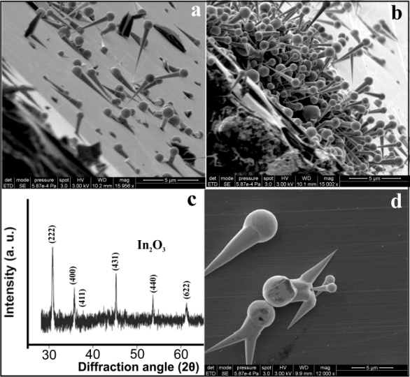
Berardan D, Guilmeau E, Maignan A, et al. (2008) In2O3:Ge, a promising n-type thermoelectric oxide composite. Solid State Commun 146: 97–101. doi: 10.1016/j.ssc.2007.12.033
![]() |
[7] |
Chen D, Zhang X, Lee AF (2015) Synthetic strategies to nanostructured photocatalysts for CO2 reduction to solar fuels and chemicals. J Mater Chem A 3: 14487–14516. doi: 10.1039/C5TA01592H
![]() |
[8] | Liu Q, Zhou Y, Mae et al. (2012) Synthesis of highly crystalline In2Ge2O7 (En) hybrid sub-nanowireswith ultraviolet photoluminescence emissions and their selective photocatalytic reductionof CO2into renewable fuel. RSC Adv 2: 3247–3250. |
[9] |
Kim SS, Park JY, Kim HS, et al. (2011) Temperature-controlled synthesis of In2Ge2O7 nanowires and their photoluminescence properties. J Phys D Appl Phys 44: 025502. doi: 10.1088/0022-3727/44/2/025502
![]() |
[10] | Jin C, Park S, Kim I, et al. (2014) Enhanced H2S gas-sensing properties of Pt- functionalized In2Ge207 nanowires. Appl Phys A 114: 591–595. |
[11] |
Gonkalves AP, Godart C (2014) New promising bulk thermoelectrics: intermetallics, pnictides and chalcogenides. Eur Phys J B 87: 42. doi: 10.1140/epjb/e2014-40989-3
![]() |
[12] |
Combe E, Bhame SD, Guilmeaua E, et al. (2012) Synthesis of In2-xGexO3 nanopowders for thermoelectric applications. J Mater Res 27: 500–505. doi: 10.1557/jmr.2011.386
![]() |
[13] |
Li L, Lee PS, Yan C, et al. (2010) Ultrahigh-Performance Solar-Blind Photodetectors Based on Individual Single-crystalline In2Ge2O7 Nanobelts. Adv Mater 22: 5145–5149. doi: 10.1002/adma.201002608
![]() |
[14] |
Kong XY, Ding Y, Yang R, et al. (2004) Single-Crystal Nanorings Formed by Epitaxial Self-Coiling of Polar Nanobelts. Science 303: 1348–1351. doi: 10.1126/science.1092356
![]() |
[15] |
Kirkham M, Wang ZL, Snyder RL (2008) In situ growth kinetics of ZnO nanobelts. Nanotechnology 19: 445708. doi: 10.1088/0957-4484/19/44/445708
![]() |
[16] |
Pan ZW, Dai ZR, Wang ZL (2001) Nanobelts of semiconducting oxides. Science 291: 1947–1949. doi: 10.1126/science.1058120
![]() |
[17] |
Vashioka S, Tokaynagi S (1967) Deposition of silicon nitride films by the silicon hydrazine process. J Electrochem Soc 114: 962–963. doi: 10.1149/1.2426791
![]() |
[18] | Rzhanov AV (1982) Silicon nitride in electronics. Novosibirsk: Nauka, 200. |
[19] |
Santos LB, Ribeiro CA, Capela JMV, et al. (2013) Kinetic parameters for thermal decomposition of hydrazine. J Therm Anal Calorim 113: 1209–1216. doi: 10.1007/s10973-013-2968-8
![]() |
[20] | Pakdehi S, Salim M, Rasoolzadeh M (2014) A Review on Decomposition of Hydrazine and Its Kinetics as a Novel Approach for CO-Free H2 Production. Res Appl Mech Eng 3: 21–25. |
[21] | Dirtu D, Odochian L, Pui A, et al. (2006) Thermal decomposition of ammonia. N2H4-an intermediate reaction product. Centr EurJ Chem 4: 666–673. |
[22] | Jishiashvili D, Shiolashvili Z, Makhatadze N, et al. (2015) Vapor-Solid growth of InP and Ga2O3 based composite nanowires. Eur Chem Bull 4: 24–29. |
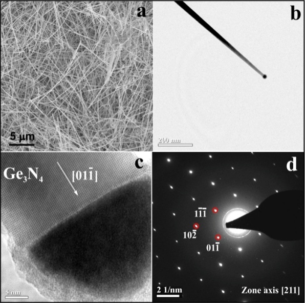
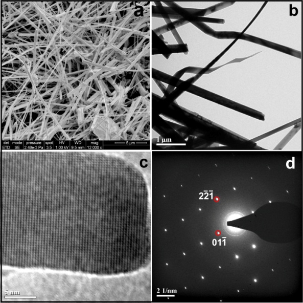
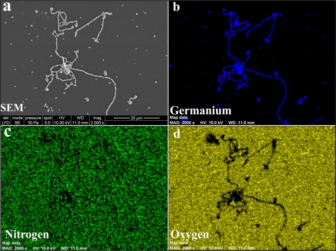
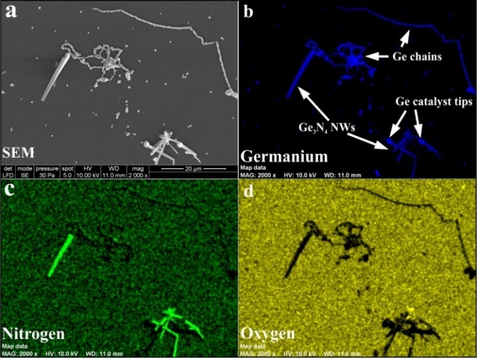
[23] | Jishiashvili D, Kiria L, Shiolashvili Z, et al. (2013) Formation of Germanium Nitride Nanowires on the Surface of Crystalline Germanium. J Nanosci 2013: 10. |
[24] | Saleem U, Wang H, Peyrot D, et al. (2016) Germanium-catalyzed growth of single-crystal GaN nanowires. J Cryst Growth 439: 28–32. |
[25] | Jumidali MM, Hashim MR, Sulieman KM (2010) Germanium catalyzed amorphous silicon dioxide nanowire synthesized via thermal evaporation method. International Conference on Enabling Science and Nanotechnology (ESciNano), Kuala Lumpur (1–3 Dec. 2010): 1–2. |
[26] | Pan ZW, Dai Sh, Rouleau CM, et al. (2005) Germanium-Catalyzed Growth of Zinc Oxide Nanowires: A Semiconductor Catalyst for Nanowire Synthesis. Angewandte Chem 117: 278–282. |
[27] |
Gu Z, Liu F, Howe JY, et al. (2009) Germanium-catalyzed hierarchical Al2O3 and SiO2 nanowire bunch arrays. Nanoscale 1: 347–354. doi: 10.1039/b9nr00040b
![]() |
[28] | Mullin JW (2001) Crystallization. Woburn: Reed Edu. & Prof. Publ. Ltd. |
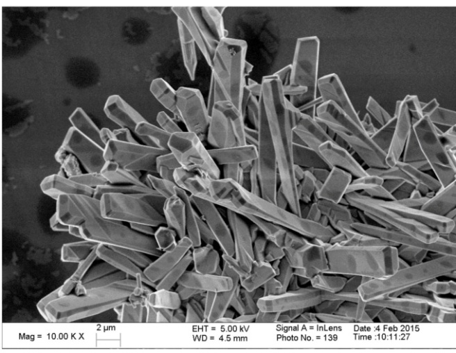
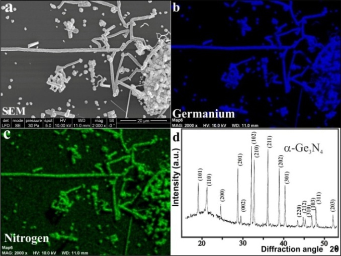
[29] | Gao YH, Bando Y, Sato T (2001) Nanobelts of the dielectric material Ge3N4. Appl Phys Lett 79: 4565–4567. |
[30] | Xie T, Jiang Z, Wu G, et al. (2005) Characterization and growth mechanism of germanium nitride nanowires prepared by an oxide-assisted method. J Cryst Growth 283: 286–290. |
[31] | Stoica T, Meijers R, Calarco R, et al. (2006) MBE growth optimization of InN nanowires. J Cryst Growth 290: 241–247. |
[32] | Denker C, Malindretos J, Werner F, et al. (2008) Self-organized growth of InN-nanocolumns on p-Si(111) by MBE. Phys Stat Solidi (C) 5: 1706–1708. |
[33] |
Goff LE, Powell REL, Kent AJ, et al. (2014) Molecular beam epitaxy of InN nanorods on Si- and C-faces of SiC substrates. J Cryst Growth 386: 135–138. doi: 10.1016/j.jcrysgro.2013.09.049
![]() |
[34] |
Cai ZM, Ye F, Jing SY, et al. (2008) A systematic study of chemical vapor deposition growth of InN. Appl Surf Sci 255: 2153–2158. doi: 10.1016/j.apsusc.2008.07.051
![]() |
[35] |
Kao M, Erasmus RM, Moloto N, et al. (2015) UV-assisted synthesis of indium nitride nano and microstructures. J Mater Chem A 3: 5962–5970. doi: 10.1039/C4TA06848C
![]() |
[36] |
Rafique S, Han L, Zhao H (2015) Chemical vapor deposition of m-plane and c-plane InN nanowires on Si (100) substrate. J Cryst Growth 415: 78–83. doi: 10.1016/j.jcrysgro.2014.12.039
![]() |
[37] |
Madapu KK, Dhara S, Polaki S, et al. (2015) Growth of InN quantum dots to nanorods: a competition between nucleation and growth rates. Cryst Eng Comm 17: 3139–3147. doi: 10.1039/C5CE00053J
![]() |
[38] |
Tian W, Zhi C, Zhai T, et al. (2012) Ultrahigh quantum efficiency of CuO nanoparticle decorated In2Ge207 nanobelt deep-ultraviolet photodetectorst. Nanoscale 4: 6318–6324. doi: 10.1039/c2nr31791e
![]() |
[39] |
Liu Z, Huang H, Liang B, et al. (2012) Zn2GeO4 and In2Ge2O7 nanowire mats based ultraviolet photodetectors on rigid and flexible substrates. Opt Express 20: 2982–2991. doi: 10.1364/OE.20.002982
![]() |
[40] |
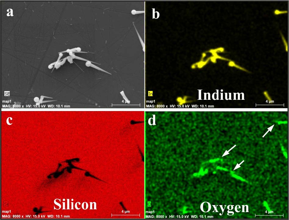
Yan C, Singh N, Lee PS (2009) Morphology Control of Indium Germanate Nanowires, Nanoribbons and Hierarchical Nanostructures. Cryst Growth Design 9: 3697–3701. doi: 10.1021/cg900406d
![]() |
[41] | Chaoyi Y, See LP (2010) Synthesis of One-dimensional (ID) Ge-based Ternary Oxide Nanostructures. Nanoelectronics Conference (I NEC) Hong Kong: 408–409. |
[42] | Zhan J, Bando Y, Hu J, et al. (2006) Hollow and polygonous microtubes of monocrystalline Indium Germanate. Angew Chem Int Ed 45: 228–231. |
[43] | Bukowski TJ (2002) The optical and photoconductive response in germanium quantum dots and indium tin oxide composite thin film structures. Thesis. University of Florida. |
[44] | Sarkisov PD (1971) Neorg Mater 7: 341–345. |
[45] |
Karazhanov SZ, Ravindran P, Grossner U (2011) First-principles study on electronic structure, phase stability, and optical properties of In2X2O7 (X═C, Si, Ge or Sn). Thin Solid Films 519: 6561–6567. doi: 10.1016/j.tsf.2011.04.221
![]() |
[46] |
Li H, Li Y, Li N, et al. (2015) A comparative study of high pressure behaviors of pyrochlore-type and thortveitite-type In2Ge2O7. RSC Adv 5: 44121–44127. doi: 10.1039/C5RA04587H
![]() |
1. | Haoyu Wang, Hongkun Huang, Teng Ma, Hao Qiang, Preparation of Zn2GeO4 semiconductor and its performance of UV detection, 2025, 09253467, 116968, 10.1016/j.optmat.2025.116968 |