Review

The role of oxygen vacancies on resistive switching properties of oxide materials

  • Tuning the level of oxygen vacancies in metal oxide materials is a promising approach to enhance resistive switching properties towards memory applications. To comprehensively understand the microstructure and oxygen vacancy migration mechanism of oxide materials, recent research in controlling the concentration of oxygen vacancies and the relationship between oxygen vacancy and resistive switching behavior as well as computational study have been reviewed in this work. In particular, the role of oxygen vacancies on the resistive switching properties of various metal oxides, including transition oxides, perovskite oxides and complex oxides are discussed in this review. Moreover, different types of processing methodologies of oxygen vacant oxide materials are reviewed and compared in detail. In the end, the future trends in fine tuning the level of oxygen vacancies are reviewed and discussed.

    Citation: Hang Meng, Shihao Huang, Yifeng Jiang. The role of oxygen vacancies on resistive switching properties of oxide materials[J]. AIMS Materials Science, 2020, 7(5): 665-683. doi: 10.3934/matersci.2020.5.665

    Related Papers:

    [1] Jens Bürger, Alireza Goudarzi, Darko Stefanovic, Christof Teuscher . Computational capacity and energy consumption of complex resistive switch networks. AIMS Materials Science, 2015, 2(4): 530-545. doi: 10.3934/matersci.2015.4.530
    [2] Timur Zinchenko, Ekaterina Pecherskaya, Dmitriy Artamonov . The properties study of transparent conductive oxides (TCO) of tin dioxide (ATO) doped by antimony obtained by spray pyrolysis. AIMS Materials Science, 2019, 6(2): 276-287. doi: 10.3934/matersci.2019.2.276
    [3] Mihaela Girtan, Laura Hrostea, Mihaela Boclinca, Beatrice Negulescu . Study of oxide/metal/oxide thin films for transparent electronics and solar cells applications by spectroscopic ellipsometry. AIMS Materials Science, 2017, 4(3): 594-613. doi: 10.3934/matersci.2017.3.594
    [4] Shuhan Jing, Adnan Younis, Dewei Chu, Sean Li . Resistive Switching Characteristics in Electrochemically Synthesized ZnO Films. AIMS Materials Science, 2015, 2(2): 28-36. doi: 10.3934/matersci.2015.2.28
    [5] Na Ta, Lijun Zhang, Qin Li . Research on the oxidation sequence of Ni-Al-Pt alloy by combining experiments and thermodynamic calculations. AIMS Materials Science, 2024, 11(6): 1083-1095. doi: 10.3934/matersci.2024052
    [6] Ming-Liang Liao . Influences of vacancy defects on tensile failure of open-tip carbon nanocones. AIMS Materials Science, 2017, 4(1): 178-193. doi: 10.3934/matersci.2017.1.178
    [7] Yustina M Pusparizkita, Vivi A. Fardilah, Christian Aslan, J. Jamari, Athanasius P Bayuseno . Understanding of low-carbon steel marine corrosion through simulation in artificial seawater. AIMS Materials Science, 2023, 10(3): 499-516. doi: 10.3934/matersci.2023028
    [8] Nirmala Kumari, Ravindra N. Singh . Nanocomposites of nitrogen-doped graphene and cobalt tungsten oxide as efficient electrode materials for application in electrochemical devices. AIMS Materials Science, 2016, 3(4): 1456-1473. doi: 10.3934/matersci.2016.4.1456
    [9] Chunsheng Wen, Xiaojiao Yu, Wei Zeng, Shan Zhao, Lin Wang, Guangchao Wan, Shicheng Huang, Hannah Grover, Zi Chen . Mechanical behaviors and biomedical applications of shape memory materials: A review. AIMS Materials Science, 2018, 5(4): 559-590. doi: 10.3934/matersci.2018.4.559
    [10] R.A. Silva, C.O. Soares, R. Afonso, M.D. Carvalho, A.C. Tavares, M.E. Melo Jorge, A. Gomes, M.I. da Silva Pereira, C.M. Rangel . Synthesis and electrocatalytic properties of La0.8Sr0.2FeO3−δ perovskite oxide for oxygen reactions. AIMS Materials Science, 2017, 4(4): 991-1009. doi: 10.3934/matersci.2017.4.991
  • Tuning the level of oxygen vacancies in metal oxide materials is a promising approach to enhance resistive switching properties towards memory applications. To comprehensively understand the microstructure and oxygen vacancy migration mechanism of oxide materials, recent research in controlling the concentration of oxygen vacancies and the relationship between oxygen vacancy and resistive switching behavior as well as computational study have been reviewed in this work. In particular, the role of oxygen vacancies on the resistive switching properties of various metal oxides, including transition oxides, perovskite oxides and complex oxides are discussed in this review. Moreover, different types of processing methodologies of oxygen vacant oxide materials are reviewed and compared in detail. In the end, the future trends in fine tuning the level of oxygen vacancies are reviewed and discussed.


    Recently, the technological advances in integrated circuits (ICs) have enabled the rapid development of modern electronic devices, such as memory devices and transistors, which has dramatically changed our daily life. However, since the IC complexity evolves exponentially and the integrated device density will face physical limit soon according to Moore’s Law, significant studied has been conducted to develop next generation electronic devices as an alternative to replace conventional ones, in order to achieve continued miniaturization of devices and development of information technology [1,2].

    More recently, resistive switching effect in various materials, where high resistance state (HRS) as well as low resistance state (LRS) can be reversely altered under an external electric field, has attracted tremendous research interest. The resistive switching devices with an inherent memory, also called memristors (memory + resistor), have been widely reported [3]. Compared with conventional memory devices, excellent switching performances, including high scalability, fast operation speed, low power consumption, excellent retention along with multibit operation capability have been demonstrated in a wide range of devices, indicating potential applications for non-volatile memory (NVM). On the other hand, based on conventional von Neumann architecture, today’s computers typically comprise separated central processing unit and memory unit, and high costs are generated during data transfer between the units. However, as resistive switching memory can be readily integrated into processor chips, thus the undesired data movements between the processor and the memory in conventional computing devices can be avoided. Furthermore, a high level of parallelism is also reported in resistive switching memory, allowing highly efficient data processing with ability to handle complex tasks, which can mimic the function of human brain. Accordingly, resistive switching devices have been further utilized to act as artificial synapses for implementation of neuromorphic computing devices, which is considered as an alternative approach to the Von Neumann computing [2,3,4,5,6].

    Resistive switching device usually possesses a simple 2-terminal, metal-insulator-metal (MIM) configuration (vertical or planar structure), in which an insulator layer as switching medium is sandwiched between two metal electrodes. In general, the switching layer acts as an electrolyte for ions migration, and a variety of metal oxides (e.g., binary oxides, ZnO, TiO2, SnO2 perovskite oxides, SrTiO3, BaTiO3, and complex oxides) have been used owing their low fabrication cost, compatibility with complementary metal-oxide semiconductor (CMOS) technology, excellent thermal stability and mechanical properties [7,8]. In most cases, they are also transparent, which shows potential applications in transparent electronic devices. The bandgap of these materials can also be tuned by defects engineering. Beyond traditional thin film structures from physical and solution processes, single nanoisland [9] and one-dimensional (1D) nanostructures (e.g., nanowire, nanotube, nanobelt) [10,11,12,13] have been used as switching materials to study their switching effects, which is beneficial for understanding the origin of switching behaviours due to the confined dimension and simplified system. Furthermore, low operation current and high density can be readily achieved in these memory devices, allowing reduced power consumption and further miniaturization of the chips [14].

    The resistive switching properties of oxides can be affected significantly by defects because the charge carrier transport behaviors remarkably depend on the defect structures. Non-stoichiometric defects, such as oxygen vacancies in metal oxide play critical roles in resistive switching. This is because these defects not only act as solid electrolyte for the ions migration, but also take part in the accompanied redox reactions, giving rise to valence change phenomenon. Specifically, when a positive voltage is applied to one electrode, the positively charged defects, such oxygen vacancies are repelled and moved to another electrode, and accordingly, oxygen-deficient and oxygen-rich regions are formed in the medium. After the oxygen vacancies are continuously piled up, the filament composed of oxygen vacancies are finally generated, and set process is realized as expected. Upon application of a negative voltage, then oxygen vacancies migrate in the opposite direction and recombine with the oxygen ions, leading to dissolved filament and reset process [2,15]. Therefore, in many cases, oxygen vacancies determine the resistive switching process and the performance of the memory devices.

    In this review, the electronic structure of the oxygen vacancies, recent efforts on controlling the concentration of oxygen vacancies and their roles on resistive switching properties are analyzed and discussed.

    Recently, first principles calculations based on density functional theory (DFT) have been used to study the implications of the formation energy and charge states of oxygen vacancy on the switching mechanisms observed in memory devices [16,17]. Oxygen vacancies and other ionic defects can be introduced in the systems and the resulting structural and energy changes can be monitored. For memory devices, it is important to determine the formation energy of oxygen vacancies near the oxide-electrode interface, and to evaluate the feasibility of the migration of oxygen vacancies under electric fields. A new method, namely climbing image nudged elastic band can be used for analyzing the migration of oxygen vacancies. This method allows for the determination of the most probable ionic diffusion paths and estimation of the accompanying kinetic energy barriers. Thus the first-principles calculations can provide atomistic guidance for tuning the resistive switching properties, as those are dominated by the concentration and mobility of ionic defects near the interfaces [18,19].

    For metal oxides, it is generally believed that the electronic structure of the transition metal atoms is affected by the on-site Coulomb interactions among the electrons in d orbitals, and sometimes in p orbitals of O for some systems such as TiO2 [20,21]. There have been some studies reported that all valence states including oxygen p orbitals must apply to self-interaction correction to get the best fit value of band gap energy compared with the experimental one. Specifically, Figure 1 shows schematics of band structure of the rutile TiO2 using Linear Discriminant Analysis (LDA) + U method. As seen, valence states including oxygen can produce the closest value of bandgap energy of rutile TiO2 to the experimental value of 3.0 eV. In fact, DFT calculations can address bandgap problems of most materials, but for systems containing d electrons and f electrons, especially transition metal oxides, the traditional DFT calculations are not accurate enough when calculating the strongly correlated systems. Therefore, Hubbard (U) is applied to electrons on d or f orbitals to describe the interaction between electrons, which can correct the failure of DFT to predict correct bandgaps for strongly correlated materials.

    Figure 1.  Comparisons of calculated bandgap value with LDA, LDA + U methods. Reproduced with permission from Ref. [16].

    Sun et al. studied the electronic structure and properties of SrZrO3 (SZO) with ordered and disordered oxygen vacancies (VOs) [22]. They found that the formation of oxygen vacancy row (VO-row) leads to defect assisted conduction filament, which is the “ON”-state of SZO memory device, while the disruption of the ordered VO-row breaks the conduction filament and therefore such structure means the “OFF”-state of SZO memory, and the resistance is quite high compared with “ON” state. The formation and disruption of VO-row in the oxide can be triggered by external electric fields through electron injection and removal. It should be noted that the electrodes also greatly affects these processes, because active metals can be oxidized and reduced and they may have lower activation energy compared with the formation and disruption of VO. Therefore for simulation the role of the electrodes should be considered.

    Oxygen vacancy (Vo) is one of the most common defects in semiconductor materials, especially in metal oxide semiconductor, which has an important impact on the properties of semiconductor materials. VOs refer to the oxygen atoms (oxygen ions) separation in the lattice of metal oxide or other oxygen-containing compounds, resulting in oxygen loss and formation of vacancy. Consequently, plenty of the studies have been performed on its role on resistive switching in oxide materials during the past decade. For example, Li et al. have evidently suggested that VOs are distributed uniformly in different oxide films. On the other hand, excessive VOs in the oxide layer only acts as a VOs reservoir themselves, which means the properties of RS can greatly influence by the concentrations of VOs [23,24]. Up to now, a couple of methods have been employed to adjust the lattice structure properties of oxides to generate additional VOs, such as temperature [25], pressure [26] and reducing gas atmosphere sintering [27]. However, it remains a challenge to control oxygen vacancy defect via engineering the structure of oxide materials under ambient conditions. Therefore, choosing a material with a corresponding synthetic method is important for the formation and accurate control of oxygen vacancy. Furthermore, to a specific application or device, a tiny difference occurred in the lattices would lead to severe influences on the materials performance promotion or demotion.

    In the previous studies, it has been indicated that inserting dopants could alter VOs in transition metal oxide based materials. Additional studies demonstrated that p-type dopants (such as Al, Y, La) imported holes into the structure may greatly reduce the formation energy of oxygen vacancy [28,29]. Hence, VOs can be effectively obtained by element doping. At the same time, the structural expansion of material lattice due to the tensile strain which caused by the dopants are also found. From the research of Fell et al. detailed analysis of the lattice structure through X-ray diffraction may give rise to the revelation of feasible alteration of the lattice structure owing to foreign atoms introduction [30]. Figure 2 shows the introduction of a Ca2+ ion into the ZrO2 lattice produces a vacancy on the O2– sub-lattice. This substitution helps to stabilise the cubic fluorite structure of ZrO2.

    Figure 2.  Scheme of the lattice of Ca doped ZrO2.

    In terms of the impact of doping on the performance of resistance switching devices, He et al. reported on fabricating the heterostructure of Pt/Ti–Ta2O5/Pt with a polycrystalline Ta2O5 film for investigation of resistance switching properties in nonvolatile memories. The results show that in aspect of unipolar RS properties, the resistance switching of Pt/Ti–TaO5/Pt is 5000% higher than the Ta2O5, and it has significant retention behavior under continuous voltage (more than 12 h). Compared to T2O5, excellent properties are observed such as higher LRS or HRS values and higher resistance switching ratio, since Ti addition in Ti-doped Ta2O5 films can suppress the migration of oxygen vacancies via forming the inactive Ti/O-vacancy complex. Therefore, this research highlights advantages of element doping in excellent RS devices [29].

    Several techniques have been successfully employed to dope oxide-based materials to generate VOs, such as, sol-gel [31], hydrothermal [32], (plasma-assisted) chemical vapor deposition (CVD) [33,34,35,36], pulsed laser deposition (PLD) [37], chemical spray pyrolysis (CSP) [38], and atomic layer deposition (ALD) [39], etc. For high temperature methods, such as CVD and PLD, the doping efficiency is relatively high because high temperature means the dopant ions can diffuse into the oxide crystal lattice easily. On the other hand, the solid solubility of the dopants also limits the doping concentration and beyond that, second phase appears and the concentration of oxygen vacancies cannot be further tuned.

    The major challenge encountered in solution processed methods, such as sol-gel, hydrothermal and chemical bath deposition lies in doping efficiency. A lot of previous studies have shown that the tendency for dopant ions to be excluded from the oxides during crystal growth in solution, which means the formation of second phase or impurities. This is particularly true for oxides grown from aqueous solution, because it is difficult to control the kinetics in each individual reaction step. That means, simple addition of dopants to the solution hardly results in incorporation of dopants in oxide crystal lattices. Hosono et al. reported the fabrication of Al doped ZnO films through the pyrolytic transformation (500 ℃) of AlCl3-added layered hydroxide zinc acetate self-templates, in the absence of seed layer [40]. They used non-aqueous system that allows water act only as a reactant in the chemical reactions. An alternative way, electrodeposition has been proved to be successfully doping Co and Ni into ZnO nanowires, which can be conducted on a conductive substrate. For electrodeposition, the nucleation and growth of oxide crystals are determined by applied currents, therefore, the dopant ions can be adsorbed on the nuclei of oxide and incorporated into the crystal lattice. Another thing needs to be considered for electrodeposition is that the doping concentration is still low due to the low temperature (<100 ℃) of electrodeposition process. Another effective method is solvo-thermal, where relatively high temperature (~200 ℃) is applied and the dopant ions have higher diffusion coefficient compared with electrodeposition process. Different form hydrothermal process, the hydrolysis of metal ions in organic solvents is much slower and the dopant ions can be incorporated into crystal lattice instead of forming second phase.

    In a recent study, the lattice structure of oxide materials might be tuned by the exposure time to a source of irradiations such as ultraviolet lamps or microwave reactors. It is worth noting that the lattice system changes may result from the variation of the VO concentrations directly (Figure 3), since the doping process as aforementioned is a practical method for the confirmation. A better understanding of the band theory of oxides will ideally service for describing further related discoveries, because of the tight relations between materials lattice structure and electronic band structure [41,42,43].

    Figure 3.  Scheme of the local atomic relaxations around the oxygen vacancy in the (a) neutral, (b) mono-charge state and (c) bi-charge states, respectively. Reprinted with permission from Ref. [42].

    Up to date, irradiation treatment, especially the microwave irradiation, has brought in an enormous amount of research interests because it is one of the most effective approaches to control the VOs creation [41,44,45]. A very recent review paper published by Kabongo et al. thorough summarized that the generation of VOs in transition metal oxide based materials assisted by microwave irradiation [46]. It should be noted that though irradiation treatment has shown their benefits like shorten reaction period and enhancing heating speed, this method needs to perform with another process to reach higher efficiency collaboratively. In addition, a series of studies have shown that high-energy electrons and ions can dissociate oxygen ions and neutral atoms on the TiO2 surface, thereby generating oxygen vacancies. Because high-energy electrons and ions can open the Ti–O bond on the surface, and then remove oxygen atoms or ions oxygen vacancies are generated on the surface. Wang et al. [47] used electron beam irradiation and Ar+ bombardment to introduce oxygen vacancies on the surface of TiO2. Yim et al. [48] introduced and regulated oxygen vacancies and their concentrations on rutile TiO2 surface by electron bombardment.

    Apart from the modification during the synthesis processing, extra VOs also can be generated by thermal treatment under different atmosphere. For instance, VO-rich titanium dioxide (TiO2–x) obtained after annealing it at a particular temperature (generally higher than 400 ℃) under the oxygen-depleted condition, such as pure helium, argon, nitrogen, gas atmosphere or vacuum condition [49]. It was also reported that reductant-assisted thermal treatment enables the removing oxygen and generating oxygen vacancies simultaneously. These reductants involve from reactive metal (such as Li, Mg, Al) to reductive agent (Boron hydride). Wang et al. successfully modified the aluminothermic reaction to massively produce nonstoichiometric TiO2–x at a relatively low temperature (i.e. 300–500 ℃) [50]. The product shows extreme visible-light absorption, so-called black titania, has been proved through Raman spectroscopy and X-ray photoelectron spectroscopy that this physical property transformation of the samples caused by the VOs generation led to an amorphous surface.

    In the earlier of this year (2018), similar results in a series of metal oxides (CeO2, ZnO, SnO2) further indicated by Ou’s Group used a simple lithium reduction strategy under room-temperature [51]. The Figure 4 shows that the three peaks labelled as O1, O2 and O3 can be presented to the lattice oxygen, oxygen defects and surface adsorbed oxygen species, respectively. It is obviously to find the content of oxygen defects in all the oxides significantly increased after lithium reduction treatment. Additionally, some studies reported cerium oxide nanoparticles were exposed to a high-temperature Carbon monoxide (CO) atmosphere for thermal treatment. The X-ray Absorption Near Edge Spectroscopy (XANES) region of the spectra changes with the procession of reaction, because of the reduction of Ce4+ to Ce3+ [52,53]. The number of oxygen vacancies is controlled by this method, which is very meaningful for the design of smart nanoparticles in future.

    Figure 4.  XPS spectra of pristine and lithium reduced oxide nanoparticles. (a) ZnO, (b) SnO2, and (c) CeO2. Reprinted with permission from Ref. [51].

    In particular, creating VOs in perovskite oxides aroused the interest of Tan et al.; they mixed and ground the SrTiO3 (STO) and NaBH4 in a glove-box before annealing samples at the temperature range from 300 to 375 ℃ within 60 min under the argon gas protection [54]. The Figure 5 shows the reflectance of the pristine STO starting around 390 nm, which matches the absorption of STO band gap (3.2 eV). For comparison, an additional absorption band over 400 nm extending to infrared regions is observed for the samples after reduction. It has believed that the diverse light absorption of STO is due to the increasing concentration of VOs on the surface of STO [55]. This means the resistive switching properties can be tuned through the band gap of the oxide materials at relatively low temperature.

    Figure 5.  UV-vis diffuse reflectance spectra of different STO samples. Adapted with permission from Ref. [54].

    By an approach of mechanochemical force, which is a common ball milling (BM) method, mechanical shearing force and pressure are applied to the ball milled powder to introduce a large amount of lattice distortion in the powder, which leads to that oxygen atoms are separated from the original lattice position and oxygen vacancies are introduced. Yang et al. used a planetary ball mill to implement mechanochemical forces to introduce oxygen vacancies on the surface of MnO2 for synthesized MnOx [56]. And the same study also confirmed that mechanochemical forces can introduce oxygen vacancies in oxides.

    Resistive switching (RS) was discovered in 1960s in oxides sandwiched between metal electrodes [57,58]. It had been realized that this effect was promising for non-volatile memory applications [59]. Since then resistive switching phenomena has puzzled a lot of scientists. In the past few decades, researchers had an improved comprehension of the mechanism of the RS. Meanwhile, unipolar and bipolar RS performances have been discovered in several classes of materials. Among them, oxides are the largest family of candidates. Herein, we focus on the switching model based on the metal-oxide-metal (MOM) structure is typically resulted by the drift-diffusion of VOs or oxygen ions. The regular viewpoint of MOM structured RS device is that the migration of VOs plays an essential role for the RS behaviour.

    Fundamentally, two categories were built for the explanation of the RS mechanism in the VCM-type devices (Scheme illustrates in the Figure 6). On the one hand, the formation/rupture of the conductive filament is caused by the interconnected/disconnected VOs by applying different voltages. On the other hand, the RS cell is dominated by the interfaces, where the switching happens at the interface near the electrode and the oxide [60,61]. Interestingly, in some practical experiments, the above switching modes can be realized in one system, which indicate that the in-depth study remain necessary to clarify the differences [62]. For simplicity, we divided oxides into three types: transition metal oxide (TMO), perovskite oxide (PO), and complex oxide (CO) to discuss the RS behaviour linked with VOs.

    Figure 6.  Classification and illustrations of the reported RS mechanisms for filamentary VCM (a), interface VCM (b); the arrows show the migration of oxygen vacancies under device operation.

    Nowadays, the resistive switching effect is one of the best-known phenomena in complex oxide-based heterostructures proposed for a novel memory cell. A lot of scientists and engineers are engaged in studies and applications of the resistive switching. Presently, some plausible models for resistive switching in oxides have been reported [6,7,8]. Among them is the voltage-enhanced oxygen-vacancy migration model (VEOVM) for bipolar resistive switching [9].

    Although the first VCM-type RS phenomenon had been observed at the 1960s in a Nb/NbOx-based cell, the research about the improvement of the NVM in the TMO family has not prevailed until the past twenty years [63]. It should be noted that the performances of the VCM RRAMs have been dramatically developed to reaching the manufacture levels recently. In TMOs, the mobility of VOs is usually higher than metal cations. The distribution and concentration of VOs would affect the valence states of the metal cations effectively. Therefore, it is vital to make the role of VOs movement clear in TMO based RS devices. In this case, several characterization approaches have been conducted to monitor the migration of VOs in the RS process. Yoshida et al. firstly reported the direct observation of VOs drifted in a NiO film during RS property measurement by C-AFM [64]. The same outcome further proved by Lee et al. from Samsung Electronics Co., Ltd. using Current Sensing-AFM [65]. Moreover, in situ TEM technique was used in the Au/CeO2/Nb-STO structure to trace the VOs migration under electrical manipulation [66].

    In 2017, Rafael et al. systematically studied a series of ceria-based RS devices including their microstructures and RS performances [67]. After that, they fabricated gadolinia-doped ceria with different doping levels to obtain RS devices with the controllable concentration of VOs and designed a model to explain the relationship between VOs and RS behaviour. There is an overview of ceria-based memristive devices and their characteristics in Table 1 [67].

    Table 1.  Overview of ceria-based single films and multilayer structures employed as oxides in memrisitve devices, their resistive switching characteristics, and microstructures. Reorganised with permission from Ref. [67].
    Switching oxide material ROFF/RON ratio Switching voltage Electroforming Oxide microstructure Device geometry Film deposition technique
    YES No
    CeO2 10 2.8 X - Cross-plane E-beam
    10 X Epitaxial
    4 3 X - Electrodeposition
    100 1.5 X Polycrystalline Pulsed laser deposition
    500 2 Epitaxial
    1000 4 X Polycrystalline
    100’000 3 Epitaxial
    50’000 1.8 Epitaxial
    1.5 -
    40 0.6 X Polycrystalline RF-sputtering
    100 2 X -
    10’000 2 X Amorphous
    100’000 1 X Polycrystalline
    Ce1-xCoxO2 1’000 2.2 Nanorods Cross-plane Electrochemical deposition
    CeO2/La0.8Sr0.2MnO3 10’000 2 X - In-plane Atomic layer deposition
    Ce0.9Gd0.1O1.95/Er2O3 15 200 X Oriented Cross-plane Pulsed laser deposition
    CeO2/La0.7(Sr0.1Ca0.9)0.3MnO3 100 4 -
    CeO2/ZnO 4’000 5 Polycrystalline

     | Show Table
    DownLoad: CSV

    Additionally, they defined VOs as “free” (mobile) or “frozen” (immobile) oxygen-deficiencies and indicated the RS enhancing would result from a high concentration of free VOs, shown in Figure 7. Their outcomes suggested that simply increasing the concentration of VOs in TMO based structure may not improve the RS performance. A link between the ionic conductivity in the oxides layer and their RS behaviour could be analogized the relations between ion diffusion and the ratio of internal VOs type (“free” vs “frozen”).

    Figure 7.  (a) and (b) represent I–V curves and schematic diagrams of the VOs migration dominant the RS properties in gadolinia-doped ceria resistive switching devices. (c) Box plot representation of the resistance ration in gadolinia-doped ceria resistive switching device units for various gadolinia concentrations. Reorganised with permission from Ref. [67].

    Generally, perovskite oxides could be simply regarded as ternary oxides with formula ABO3, where A and B represent metal cations. VOs also play a critical role in RS devices composed of PO. In order to explicate the vital physical mechanism of PO based RS, a number of models, for instance, modify the interface property induced by the motion of VOs has been proposed. By recent results, it is promising to control the PO based RS behaviour by manipulating the concentration of VOs at the interface area during the fabrication process. Jin et al. investigated the RS mechanisms in the oxygen-deficient LaMnO3 (LMO) and BiFeO3 (BFO) [68]. The migration of the VOs at the interface of these materials led to the resistance change of the devices, obtained an interface-type RS characteristic. A year later, Panda et al. selected two typical POs, SrZrO3 (SZO) and SrTiO3 (STO) as models, to thoroughly summarize the RS properties [69]. The SZO based RRAM devices have been widely accepted as show VCM filamentary type RS performance (Zr3+/Zr4+), which formation/rupture filaments made by VOs as a dominant factor for RS behaviours.

    For the STO based memory cells, especially the samples doped with iron, two types of VCM RS behaviour (filamentary and interface) can be observed in one and at the same junction by C-AFM [70]. The RS behaviour of a framework Pt/Fe:STO(500 nm)/Nb:STO is shown in Figure 8 as an I–V curve. Later, Lim et al. and Bagdzevicius et al. separately reviewed complex physical phenomena and active mechanisms which were linked to the appearance of RS in POS, together with several relevant examples for each material system [61]. They also presented some examples of conduction mechanisms explanations and summarizes related resistive switching devices based on perovskite oxides [71]. It noteworthy that several issues are not clear yet, especially for the understanding of the physicochemical effects induced RS behaviour might remain debatable in various actual cases.

    Figure 8.  (a) I–V curve of a Fe-doped STO based device. Two types of RS behaviour exhibiting opposite polarities can be seen in one and the same junction. (b) C-AFM topography and current image of a junction after electroforming and top electrode removal. Reprinted with permission from Ref. [69].

    Complex oxides contain at least three elements except for oxygen, such as PrxCa1–xMnO3 (PCMO), LaxCa1–xMnO3 (LCMO) and YBa2Cu3O7 (YBCO). Most of the CO was a perovskite-related VOs-rich material that proved promising for the modern electric device. Tarasova investigated the introduction of low concentrations of fluoride ions increases the ionic component of the conductivity [72], shown in Figure 9. Nowadays, increasingly research on the RS performance in CO-based heterostructures for proposing novel memories. A consensus has been broadly believed that the migration of VOs at the interface area of system junction was considered to be a core factor of the RS in PCMO with the Schottky-like barrier [73]. Wang et al. reported an investigation of the relationship among the configuration or concentration of VOs and RS effects in an epitaxial grown LCMO/STO structure [74]. Rearrangements of VOs diffusing to/away from CO interfaces correlate with the resistance stage changing of the LCMO based memristive device. Plecenik et al. experimentally verified the crystal growth orientation of the YBCO compound has a significant effect on their RS performance. The consequence implies a deep reason that was the fast diffusion of VOs on c-axis, which explained the observation of an asymmetric I-V curve and bipolar RS property of YBCO [75].

    Figure 9.  Raman spectra of BIOFx. Adapted with permission from Ref. [72].

    It can be summarized that CO-based RS mainly belongs to the interface-type VCM driven memory applications. Bao et al. explored the VO exchange dynamics at COs surfaces and interfaces at very recent. Their research shows a convenient way for better understanding of interfacial VOs dynamics in CO. Both PrBaCo2O5+δ (PBCO) epitaxial film which shows the ultra-fast diffusion rate of VOs under different temperatures and new approach of ionic liquid gating method [76,77] were applied in their experiment. The +/− gating voltage drives the −/+ charge carriers to gather to the surface region of PBCO film, leading to a decrease/increase of the resistance, i.e. the PBCO based device can be reversibly set/reset from the HRS to LRS, or the other direction.

    In summary, oxygen vacancy (Vo) plays a key role in determining the resistive switching behaviour of oxide materials. Computer simulation results combined with experimental studies indicate that resistive switching states between high resistance state (OFF) and low resistance state (ON) in oxide materials can be led by the density change of Vo, where Vo assisted conduction channel can result in the “ON” state of the memory device, and the disruption of the ordered Vo breaks the conduction channels and therefore turns off the memory device. Furthermore, the presence of this leading effect of Vo density can be explained by electrons capture and emission under electric field through oxygen vacancies migration. Following this idea, there have been a lot of studies focused on tuning the concentration of Vo in oxides in order to achieve desired resistive switching performance. It should be noted that there is a suitable concentration window of Vo, because too high Vo means the oxide is highly conductive, which results in low ON/OFF ratio. On the other hand, low Vo means limited mobile ions in the oxides and it is more difficult to switch ON/Off the device. In addition, it is essential to control the distribution of Vo in oxides, as this will affect the device uniformity. In summary, recent research progress has demonstrated the significance of Vo in theory and gives physical insights into the switching mechanism and also for improving the device performance.

    There are still some challenges in this area, for example, accurate and quantitative theory as well as experimental approach to identify the exact role of Vo in resistive switching are limited. Therefore, (1) new methods should be developed to monitor the generation of Vo during resistive switching process and quantify its concentration. One promising tool is 3D SIMS-SPM prototype, namely secondary ion mass spectrometry (SIMS), which the data is linked with topographical images from scanning probe microscopy (SPM) module to get accurate chemical 3D map of the oxides with and without external electric field. This is particularly important for thin film devices as it is difficult to identify the oxygen vacancy distribution in thin film by conventional characterization technologies. (2) It would be interesting to introduce Vo at low temperature, as oxide crystals will grow and cracks will form at high temperature, and also for some specific applications, such as flexible electronics, high temperature is harmful for flexible substrates. One of the possible approaches is plasma treatment. Plasma processing can bypass the grain growth and cracks formation, and introduce Vo owing to oxygen deficient atmosphere. Different plasma treating processes, such as Ar plasma, N2 plasma need to be finely tuned to create a suitable level of oxygen vacancy without introducing other harmful structural defects which will degrade the device performance. (3) Controlling the distribution of Vo in oxide materials can further improve the device uniformity. To achieve this goal, one can tune the morphology of oxide crystals, such as nanocube, nanospheres as Vo is usually distributed on the surface of the oxide crystals and surface of Vo can easily migrate under external electric field. Other direction is to design the oxide/electrode interface with controllable oxygen diffusion barriers, which may further enhance the performance of the devices, and create new functionalities such as memristive switching, and memcapactive switching.

    The authors declare that there is no conflict of interest.


    [1] Kish LB (2002) End of Moore's law: thermal (noise) death of integration in micro and nano electronics. J Phys Lett A 305: 144-149.
    [2] Lee J, Lu WD (2018) On-demand reconfiguration of nanomaterials: When electronics meets ionics. Adv Mater 30: 1702770.
    [3] Zidan MA, Strachan JP, Lu WD (2018) The future of electronics based on memristive systems. J Nat Electron 1: 22.
    [4] Jeong DS, Thomas R, Katiyar R, et al. (2012) Emerging memories: resistive switching mechanisms and current status. Rep Prog Phys 75: 76502.
    [5] Wang Z, Wang L, Nagai M, et al. (2017) Nanoionics-enabled memristive devices: Strategies and materials for neuromorphic applications. Adv Electron Mater 3: 1600510.
    [6] Ielmini D, Wong HSP (2018) In-memory computing with resistive switching devices. Nat Electron 1: 333-343.
    [7] Wang Y, Lv Z, Zhou L, et al. (2018) Emerging perovskite materials for high density data storage and artificial synapses. J Mater Chem C 6: 1600-1617.
    [8] Ye C, Wu J, He G, et al. (2016) Physical mechanism and performance factors of metal oxide based resistive switching memory: a review. J Mater Sci Technol 32: 1-11.
    [9] Qi J, Olmedo M, Ren J, et al. (2012) Resistive switching in single epitaxial ZnO nanoislands. J ACS nano 6: 1051-1058.
    [10] Nagashima K, Yanagida T, Oka K, et al. (2010) Resistive switching multistate nonvolatile memory effects in a single cobalt oxide nanowire. J Nano Lett 10: 1359-1363.
    [11] Tan ZH, Yin XB, Guo X (2015) One-dimensional memristive device based on MoO3 nanobelt. J Appl Phys Lett 106: 23503.
    [12] Liang KD, Huang CH, Lai CC, et al. (2014) Single CuOx nanowire memristor: forming-free resistive switching behavior. ACS Appl Mater Inter 6: 16537-16544.
    [13] Huang CH, Chang WC, Huang JS, et al. (2017) Resistive switching of Sn-doped In2O3/HfO2 core-shell nanowire: geometry architecture engineering for nonvolatile memory. Nanoscale 9: 6920-6928.
    [14] Hsu CW, Chou LJ (2012) Bipolar resistive switching of single gold-in-Ga2O3 nanowire. Nano Lett 12: 4247-4253.
    [15] Li Y, Long S, Liu Q, et al. (2017) Resistive switching performance improvement via modulating nanoscale conductive filament, involving the application of two-dimensional layered materials. Small 13: 1604306.
    [16] Zhao L, Park SG, Magyari-Köpe B, et al. (2013) First principles modeling of charged oxygen vacancy filaments in reduced TiO2-implications to the operation of non-volatile memory devices. Math Computr Model 58: 275-281.
    [17] Dai Y, Pan Z, Wang F, et al. (2016) Oxygen vacancy effects in HfO2-based resistive switching memory: First principle study. AIP Adv 6: 85209.
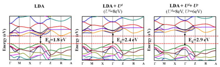
    [18] Park SG, Magyari-Köpe B, Nishi Y (2010) Electronic correlation effects in reduced rutile TiO2 within the LDA + U method. J Physical Review B 82: 115109.
    [19] Park SG, MagyariKope B, Nishi Y (2011) Impact of oxygen vacancy ordering on the formation of a conductive filament in TiO2 for resistive switching memory. IEEE Electr Device L 32: 197-199.
    [20] Park S, Magyari-Kope B, Nishi Y (2011) Theoretical study of the resistance switching mechanism in rutile TiO2-x for ReRAM: the role of oxygen vacancies and hydrogen impurities. 2011 Symposium on VLSI Technology-Digest of Technical Papers 46-47.
    [21] Park SG, Magyari-Kope B, Nishi Y (2008) First-principles study of resistance switching in rutile TiO2 with oxygen vacancy. 2008 9th Annual Non-Volatile Memory Technology Symposium 9: 1-5.
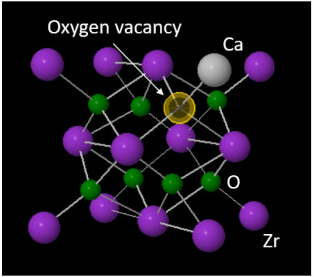
    [22] Guo Z, Sa B, Zhou J, et al. (2013) Role of oxygen vacancies in the resistive switching of SrZrO3 for resistance random access memory. J Alloys Compd 580: 148-151.
    [23] Li XM, Qi K, Sun MH, et al. (2015) Real-time observation of dynamic process of oxygen vacancy migration in cerium oxides under electric field. Appl Phys Lett 107: 211902.
    [24] Xu ZT, Jin KJ, Gu L, et al. (2012) Evidence for a crucial role played by oxygen vacancies in LaMnO3 resistive switching memories. Small 8: 1279-1284.
    [25] Miao ZL, Chen L, Zhou F, et al. (2018) Modulation of resistive switching characteristics for individual BaTiO3 microfiber by surface oxygen vacancies. J Phys D Appl Phys 51: 224-183.
    [26] Ge J, Chaker M (2017) Oxygen vacancies control transition of resistive switching mode in single-crystal TiO2 memory device. ACS Appl Mater Inter 9: 16327-16334.
    [27] Strunk J, Vining WC, Bell AT (2010) A study of oxygen vacancy formation and annihilation in submonolayer coverages of TiO2 dispersed on MCM-48. J Phys Chem C 114: 16937-16945.
    [28] Zhao L, Ryu S, Hazeghi A, et al. (2013) Dopant selection rules for extrinsic tunability of HfOx RRAM characteristics: A systematic study. 2013 Symposium on VLSI Technology T106-T107.
    [29] Jiang H, Stewart DA (2017) Using dopants to tune oxygen vacancy formation in transition metal oxide resistive memory. ACS Appl Mater Inter 9: 16296-16304.
    [30] Fell CR, Qian DN, Carroll KJ, et al. (2013) Correlation between oxygen vacancy, microstrain, and cation distribution in lithium-excess layered oxides during the first electrochemical cycle. Chem Mater 25: 1621-1629.
    [31] Zhu XJ, Zhuge F, Li M, et al. (2011) Microstructure dependence of leakage and resistive switching behaviours in Ce-doped BiFeO3 thin films. J Phys D Appl Phys 44: 415104.
    [32] Zhang P, Gao CX, Lv FZ, et al. (2014) Hydrothermal epitaxial growth and nonvolatile bipolar resistive switching behavior of LaFeO3-PbTiO3 films on Nb:SrTiO3(001) substrate. Appl Phys Lett 105: 152904.
    [33] Lei M, He HP, Yu QQ, et al. (2015) Optical properties of Na-doped ZnO nanorods grown by metalorganic chemical vapor deposition. Mater Lett 160: 547-549.
    [34] Thandavan TMK, Gani SMA, Wong CS, et al. (2015) Enhanced photoluminescence and Raman properties of Al-doped ZnO nanostructures prepared using thermal chemical vapor deposition of methanol assisted with heated brass. Plos One 10: e0121756.
    [35] Li F, Liu XC, Zhou RW, et al. (2014) Strong correlation between oxygen vacancy and ferromagnetism in Yb-doped ZnO thin films. J Appl Phys 116: 243910.
    [36] Murali A, Sohn HY (2018) Photocatalytic properties of plasma-synthesized zinc oxide and tin-doped zinc oxide (TZO) nanopowders and their applications as transparent conducting films. J Mater Sci-Mater El 29: 14945-14959.
    [37] Henning RA, Leichtweiss T, Dorow-Gerspach D, et al. (2017) Phase formation and stability in TiOx and ZrOx thin films: Extremely sub-stoichiometric functional oxides for electrical and TCO applications. Z Krist-Cryst Mater 232: 161-183.
    [38] Deepa S, Kumari KP, Thomas B (2017) Contribution of oxygen-vacancy defect-types in enhanced CO2 sensing of nanoparticulate Zn-doped SnO2 films. Ceram Int 43: 17128-17141.
    [39] Mundle R, Carvajal C, Pradhan AK (2016) ZnO/Al:ZnO transparent resistive switching devices grown by atomic layer deposition for memristor applications. Langmuir 32: 4983-4995.
    [40] Hosono E, Fujihara S, Kimura T (2004) Fabrication and electrical properties of micro/nanoporous ZnO Al films. Mater Chem 14: 881-886.
    [41] Jafta CJ, Mathe MK, Manyala N, et al. (2013) Microwave-assisted synthesis of high-voltage nanostructured LiMn1.5Ni0.5O4 spinel: tuning the Mn3+ content and electrochemical performance. ACS Appl Mater Inter 5: 7592-7598.
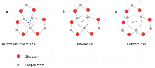
    [42] Janotti A, Van de Walle CG (2005) Oxygen vacancies in ZnO. Appl Phys Lett 87.
    [43] Janotti A, Van de Walle CG (2009) Fundamentals of zinc oxide as a semiconductor. Rep Prog Phys 72: 126501.
    [44] Kebede MA, Yannopoulos SN, Sygellou L, et al. (2017) High-voltage LiNi0.5Mn1.5O4-δ spinel material synthesized by microwave-assisted thermo-polymerization: Some insights into the microwave-enhancing physico-chemistry. J Electrochem Soc 164: A3259-A3265.
    [45] Wang J, Chen RS, Xia Y, et al. (2017) Cost-effective large-scale synthesis of oxygen-defective ZnO photocatalyst with superior activities under UV and visible light. Ceram Int 43: 1870-1879.
    [46] Kabongo GL, Ozoemena K, Dhlamini S, et al. (2018) Microwave irradiation induces oxygen vacancy in metal oxides based materials and devices: A review. J Nanosci Curr Res 3: 2-13.
    [47] Wang LQ, Baer DR, Engelhard MH, et al. (1995) The adsorption of liquid and vapor water on TiO2 (110) surfaces: the role of defects. Surf Sci 344: 237-250.
    [48] Yim CM, Pang CL, Thornton G (2010) Oxygen vacancy origin of the surface band-gap state of TiO2 (110). Phys Rev Lett 104: 036806.
    [49] Pan X, Yang MQ, Fu X, et al. (2013) Defective TiO2 with oxygen vacancies: synthesis, properties and photocatalytic applications. Nanoscale 5: 3601-3614.
    [50] Wang Z, Yang C, Lin T, et al. (2013) Visible-light photocatalytic, solar thermal and photoelectrochemical properties of aluminium-reduced black titania. Energ Environ Sci 6: 3007-3014.
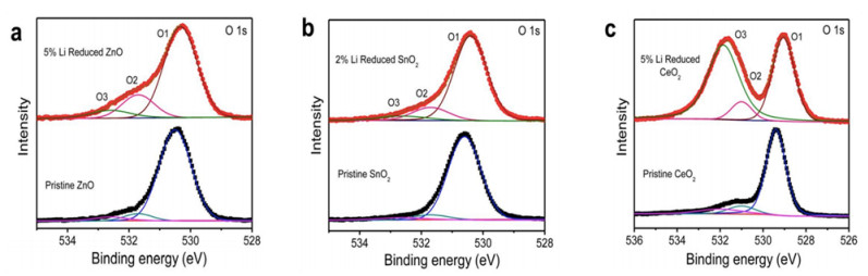
    [51] Ou G, Xu Y, Wen B, et al. (2018) Tuning defects in oxides at room temperature by lithium reduction. Nat Commun 9: 1-9.
    [52] Lawrence NJ, Brewer JR, Wang L, et al. (2011) Defect engineering in cubic cerium oxide nanostructures for catalytic oxidation. Nano lett 11: 2666-2671.
    [53] Della Mea GB, Matte LP, Thill AS, et al. (2017) Tuning the oxygen vacancy population of cerium oxide (CeO2-x, 0 < x < 0.5) nanoparticles. Appl Surf Sci 422: 1102-1112.
    [54] Tan HQ, Zhao Z, Zhu WB, et al. (2014) Oxygen vacancy enhanced photocatalytic activity of pervoskite SrTiO3. ACS Appl Mater Inter 6: 19184-19190.
    [55] Tan HQ, Zhao Z, Niu M, et al. (2014) A facile and versatile method for preparation of colored TiO2 with enhanced solar-driven photocatalytic activity. Nanoscale 6: 10216-10223.
    [56] Yang Y, Zhang S, Wang S, et al. (2015) Ball milling synthesized MnOx as highly active catalyst for gaseous POPs removal: significance of mechanochemically induced oxygen vacancies. Environ Sci Technol 49: 4473-4480.
    [57] Hickmott TW (1962) Low-frequency negative resistance in thin anodic oxide films. J Appl Phys 33: 2669-2682.
    [58] Gibbons JF, Beadle WE (1964) Switching properties of thin Nio films. Solid State Electron 7: 785-790.
    [59] Nielsen PH, Bashara NM (1964) Reversible voltage-induced initial resistance in negative resistance sandwich structure. IEEE T Electron Dev 11: 243-244.
    [60] Tian XZ, Wang LF, Li XM, et al. (2013) Recent development of studies on the mechanism of resistive memories in several metal oxides. Sci China Phys Mech 56: 2361-2369.
    [61] Bagdzevicius S, Maas K, Boudard M, et al. (2017) Interface-type resistive switching in perovskite materials. J Electroceram 39: 157-184.
    [62] Qi J, Olmedo M, Zheng JG, et al. (2013) Multimode resistive switching in single ZnO nanoisland system. Sci Rep 3: 2405.
    [63] Hiatt WR, Hickmott TW (1965) Bistable switching in niobium oxide diodes. Appl Phys Lett 6: 106-108.
    [64] Yoshida C, Kinoshita K, Yamasaki T, et al. (2008) Direct observation of oxygen movement during resistance switching in NiO/Pt film. Appl Phys Lett 93: 042106.
    [65] Lee MJ, Han S, Jeon SH, et al. (2009) Electrical manipulation of nanofilaments in transition-metal oxides for resistance-based memory. Nano Lett 9: 1476-1481.
    [66] Gao P, Wang ZZ, Fu WY, et al. (2010) In situ TEM studies of oxygen vacancy migration for electrically induced resistance change effect in cerium oxides. Micron 41: 301-305.
    [67] Schmitt R, Spring J, Korobko R, et al. (2017) Design of oxygen vacancy configuration for memristive systems. ACS Nano 11: 8881-8891.
    [68] Jin YL, Jin KJ, Ge C, et al. (2013) Resistive switching phenomena in complex oxide heterostructures. Mod Phys Lett B 27: 1330021.
    [69] Panda D, Tseng TY (2014) Perovskite oxides as resistive switching memories: A review. Ferroelectrics 471: 23-64.
    [70] Muenstermann R, Menke T, Dittmann R, et al. (2010) Coexistence of filamentary and homogeneous resistive switching in Fe-doped SrTiO3 thin-film memristive devices. Adv Mater 22: 4819-4822.
    [71] Lim EW, Ismail R (2015) Conduction mechanism of valence change resistive switching memory: A survey. Electronics 4: 586-613.
    [72] Tarasova NA (2020) Effect of fluorine doping on the ionic (O2-, H+) conductivity of oxygen-deficient complex oxides. Russ Chem B 69: 1253-1263.
    [73] Sawa A (2008) Resistive switching in transition metal oxides. Mater Today 11: 28-36.
    [74] Wang ZH, Yang Y, Gu L, et al. (2012) Correlation between evolution of resistive switching and oxygen vacancy configuration in La0.5Ca0.5MnO3 based memristive devices. Nanotechnology 23: 265202.
    [75] Plecenik T, Tomasek M, Belogolovskii M, et al. (2012) Effect of crystallographic anisotropy on the resistance switching phenomenon in perovskites. J Appl Phys 111: 056106.
    [76] Choi JH, Xie W, Gu YY, et al. (2015) Single ion conducting, polymerized ionic liquid triblock copolymer films: High capacitance electrolyte gates for n-type transistors. ACS Appl Mater Inter 7: 7294-7302.
    [77] Lu N, Zhang P, Zhang Q, et al. (2017) Electric-field control of tri-state phase transformation with a selective dual-ion switch. Nature 546: 124-128.
  • This article has been cited by:

    1. C. Dharanya, Gnanaprakash Dharmalingam, Oxygen vacancies in nanostructured hetero-interfacial oxides: a review, 2022, 24, 1388-0764, 10.1007/s11051-022-05440-4
    2. Muhammad Ismail, Chandreswar Mahata, Myounggon Kang, Sungjun Kim, Robust Resistive Switching Constancy and Quantum Conductance in High-k Dielectric-Based Memristor for Neuromorphic Engineering, 2022, 17, 1556-276X, 10.1186/s11671-022-03699-z
    3. Sobia Ali Khan, Mehr Khalid Rahmani, Muhammad Umair Khan, Jungmin Kim, Jinho Bae, Moon Hee Kang, Multistate Resistive Switching with Self-Rectifying Behavior and Synaptic Characteristics in a Solution-processed ZnO/PTAA Bilayer Memristor, 2022, 169, 0013-4651, 063517, 10.1149/1945-7111/ac7754
    4. Muhammad Ismail, Maria Rasheed, Sunghun Kim, Chandreswar Mahata, Myounggon Kang, Sungjun Kim, Unveiling the Potential of HfO2/WS2 Bilayer Films: Robust Analog Switching and Synaptic Emulation for Advanced Memory and Neuromorphic Computing, 2023, 5, 2639-4979, 3080, 10.1021/acsmaterialslett.3c00600
    5. Mir Waqas Alam, Ayangla Jamir, Bendangchila Longkumer, Basma Souayeh, Shima Sadaf, Borish Moirangthem, Bipolar resistive switching behavior of bilayer β-Ga2O3/WO3 thin film memristor device, 2025, 1010, 09258388, 177032, 10.1016/j.jallcom.2024.177032
    6. Ipek Efe, Bixin Yan, Morgan Trassin, Engineering of ferroelectricity in thin films using lattice chemistry: A perspective, 2024, 125, 0003-6951, 10.1063/5.0232382
    7. Ya-Qi Chen, Zheng-Hua Tang, Chun-Zhi Jiang, De-Gao Xu, Resistive switching properties of SnO2 nanowires fabricated by chemical vapor deposition, 2023, 32, 1674-1056, 097302, 10.1088/1674-1056/acc3fd
    8. Mingchao Zhang, Hui Chen, Kang Cheng, Liangqun Zhao, Hengliang Huang, Jincan Kang, Qinghong Zhang, Ye Wang, Reaction-Induced Formation of CoOx–InOx Interfaces for the Hydrogenation of CO2 to Methanol, 2025, 1932-7447, 10.1021/acs.jpcc.4c08481
    9. Asutosh Patnaik, Debashis Panda, Ping-Xing Chen, Narayan Sahoo, Tseung-Yuen Tseng, Metal free all oxide SnOx/HfOx bilayer transristor synapse for neuromorphic computing, 2025, 137, 0021-8979, 10.1063/5.0231295
    10. Xiaoya Ding, Shanshan Dang, Wenqiang Zhang, Xiaolu Ni, Changlong Zhang, Zhenzhou Zhang, Weifeng Tu, Co promotion of In2O3 for selective hydrogenation of CO2 to methanol, 2025, 582, 24688231, 115206, 10.1016/j.mcat.2025.115206
  • Reader Comments
  • © 2020 the Author(s), licensee AIMS Press. This is an open access article distributed under the terms of the Creative Commons Attribution License (http://creativecommons.org/licenses/by/4.0)
通讯作者: 陈斌, bchen63@163.com
  • 1. 

    沈阳化工大学材料科学与工程学院 沈阳 110142

  1. 本站搜索
  2. 百度学术搜索
  3. 万方数据库搜索
  4. CNKI搜索

Metrics

Article views(7861) PDF downloads(672) Cited by(10)

Figures and Tables

Figures(9)  /  Tables(1)

Other Articles By Authors

/

DownLoad:  Full-Size Img  PowerPoint
Return
Return

Catalog