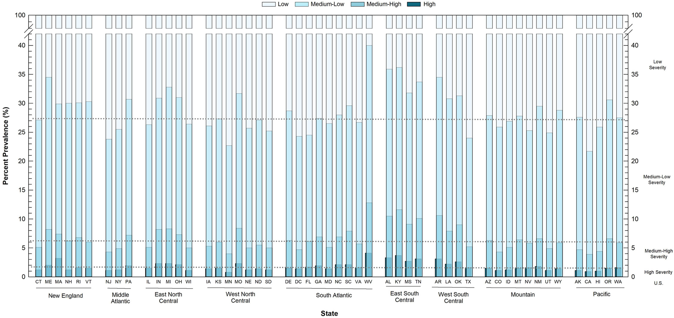
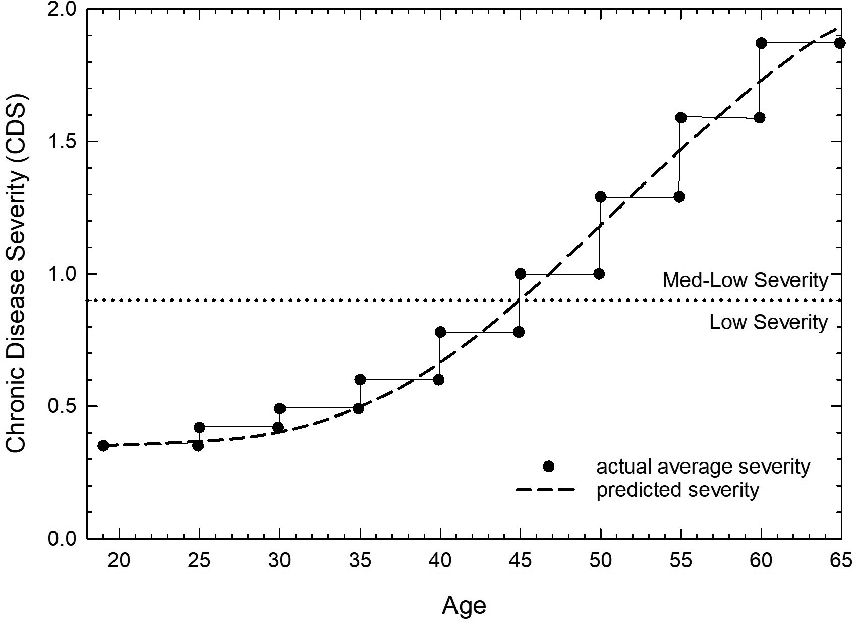
In the healthcare sector, patients can be categorized into clinical risk groups, which are based, in part, on multiple chronic conditions. Population-based measures of clinical risk groups for population health planning, however, are not available. Using responses of working-age adults (19–64 years old) from the Behavioral Risk Factor Surveillance System for survey years 2015–2017, a population-based measure of chronic disease severity (CDS) was developed as a proxy for clinical risk groups. Four categories of CDS were developed: low, medium-low, medium-high, and high, based on self-reported diagnoses of multiple chronic conditions, weighted by hospitalization costs. Prevalence estimates of CDS were prepared, by population demographics and state characteristics, and CDS association with perceived health-related quality of life (HRQOL) was evaluated. Age-adjusted CDS varied from 72.9% (95% CI: 72.7–73.1%) for low CDS, to 21.0% (95% CI: 20.8–21.2%), 4.4% (95% CI: 4.3–4.5%) and 1.7% (95% CI: 1.6–1.8%) for medium-low, medium-high, and high CDS, respectively. The prevalence of high CDS was significantly greater (p < 0.05) among older adults, those living below the federal poverty level, and those with disabilities. The adjusted odds of fair/poor perceived HRQOL among adults with medium-low or medium-high/high CDS were 2.39 times (95% CI: 2.30–2.48) or 6.53 times (95% CI: 6.22–6.86) higher, respectively, than adults with low CDS. Elevated odds of fair/poor HRQOL with increasing CDS coincided with less prevalence of high CDS among men, minority race/ethnicities, and adults without insurance, suggesting a link between CDS and risk of mortality. Prevalence of high CDS was significantly higher (p < 0.05) in states with lower population density, lower per capita income, and in states that did not adopt the ACA. These results demonstrate the relevance of a single continuous population-based measure of chronic disease severity for health planning at the state, regional, and national levels.
Citation: Carol L. Stone. A population-based measure of chronic disease severity for health planning and evaluation in the United States[J]. AIMS Public Health, 2020, 7(1): 44-65. doi: 10.3934/publichealth.2020006
In the healthcare sector, patients can be categorized into clinical risk groups, which are based, in part, on multiple chronic conditions. Population-based measures of clinical risk groups for population health planning, however, are not available. Using responses of working-age adults (19–64 years old) from the Behavioral Risk Factor Surveillance System for survey years 2015–2017, a population-based measure of chronic disease severity (CDS) was developed as a proxy for clinical risk groups. Four categories of CDS were developed: low, medium-low, medium-high, and high, based on self-reported diagnoses of multiple chronic conditions, weighted by hospitalization costs. Prevalence estimates of CDS were prepared, by population demographics and state characteristics, and CDS association with perceived health-related quality of life (HRQOL) was evaluated. Age-adjusted CDS varied from 72.9% (95% CI: 72.7–73.1%) for low CDS, to 21.0% (95% CI: 20.8–21.2%), 4.4% (95% CI: 4.3–4.5%) and 1.7% (95% CI: 1.6–1.8%) for medium-low, medium-high, and high CDS, respectively. The prevalence of high CDS was significantly greater (p < 0.05) among older adults, those living below the federal poverty level, and those with disabilities. The adjusted odds of fair/poor perceived HRQOL among adults with medium-low or medium-high/high CDS were 2.39 times (95% CI: 2.30–2.48) or 6.53 times (95% CI: 6.22–6.86) higher, respectively, than adults with low CDS. Elevated odds of fair/poor HRQOL with increasing CDS coincided with less prevalence of high CDS among men, minority race/ethnicities, and adults without insurance, suggesting a link between CDS and risk of mortality. Prevalence of high CDS was significantly higher (p < 0.05) in states with lower population density, lower per capita income, and in states that did not adopt the ACA. These results demonstrate the relevance of a single continuous population-based measure of chronic disease severity for health planning at the state, regional, and national levels.

| [1] |
Buttorff C, Ruder T, Bauman M (2017) Multiple chronic conditions in the United States Santa Monica, CA: RAND. doi: 10.7249/TL221

|
| [2] |
DeSalvo KB, Jones TM, Peabody J, et al. (2009) Health care expenditure prediction with a single item, self-rated health measure. Med Care 47: 440-447. doi: 10.1097/MLR.0b013e318190b716
|
| [3] | U.S. Department of Health and Human Services (2010) Multiple chronic conditions—a strategic framework: optimum health and quality of life for individuals with multiple chronic conditions, 2010.Available from: https://www.hhs.gov/sites/default/files/ash/initiatives/mcc/mcc_framework.pdf. |
| [4] | Averill RF, Goldfield NI, Eisenhandler J, et al. (1999) Development and evaluation of clinical risk groups (CRGs). Document No.: 9-99.Available from: https://pdfs.semanticscholar.org/505e/db4f2cf344b206aadc4a351de4ac956c9a60.pdf. |
| [5] |
Fleishman J, Cohen J (2010) Using information on clinical conditions to predict high-cost patients. Health Serv Res 45: 532-552. doi: 10.1111/j.1475-6773.2009.01080.x
|
| [6] |
Hughes JS, Averill RF, Eisenhandler J, et al. (2004) Clinical risk groups (CRGs): A classification system for risk-adjusted capitation-based payment and health care management. Med Care 42: 81-90. doi: 10.1097/01.mlr.0000102367.93252.70
|
| [7] | Winkelman R, Damler R (2008) Risk adjustment in state Medicaid programs. Health Watch 57: 14-34. Available from: https://www.soa.org/globalassets/assets/library/newsletters/health-watch-newsletter/2008/january/hsn-2008-iss57-damler-winkelman.pdf. |
| [8] |
Adams ML, Grandpre J, Katz DL, et al. (2019) The impact of key modifiable risk factors on leading chronic conditions. Prev Med 120: 113-118. doi: 10.1016/j.ypmed.2019.01.006
|
| [9] |
Newman D, Levine E, Kishore S (2019) Prevalence of multiple chronic conditions in New York State, 2011–2016. PLoS One 14: 1-16. doi: 10.1371/journal.pone.0211965
|
| [10] | Centers for Disease Control and Prevention (2019) Behavioral Risk Factor Surveillance System Atlanta, GA.Available from: https://www.cdc.gov/brfss/. |
| [11] | Chen HY, Baumgardner D, Rice J (2011) Health-related quality of life among adults with multiple chronic conditions in the United States, Behavioral Risk Factor Surveillance System, 2007. Prev Chronic Dis 8: 1-9. |
| [12] |
Hagerty MR, Cummins R, Ferriss AL, et al. (2001) Quality of life indexes for national policy: review and agenda for research. Bull Sociol Methodol 55: 58-78. doi: 10.1177/075910630107100104
|
| [13] |
Zhao G, Okoro C, Hsia J, et al. (2018) Self-perceived poor/fair health, frequent mental distress, and health insurance status among working-aged US adults. Prev Chronic Dis 15: E95. doi: 10.5888/pcd15.170523
|
| [14] |
Chanlongbutra A, Singh G, Mueller C (2018) Adverse childhood experiences, health-related quality of life, and chronic disease risks in rural areas of the United States. J Environ Public Health 2018: 1-15. doi: 10.1155/2018/7151297
|
| [15] |
White K, Lawrence JA, Cummings JL, et al. (2019) Emotional and physical reactions to perceived discrimination, language preference, and health-related quality of life among Latinos and Whites. Qual Life Res 28: 2799-2811. doi: 10.1007/s11136-019-02222-9
|
| [16] |
Zimmerman FJ, Anderson NW (2019) Trends in Health Equity in the United States by race/ethnicity, sex, and income, 1993–2017. JAMA Netw Open 2: e196386. doi: 10.1001/jamanetworkopen.2019.6386
|
| [17] |
Dube SR, Liu J, Fan AZ, et al. (2019) Assessment of age-related differences in smoking status and health-related quality of life (HRQOL): findings from the 2016 behavioral risk factor surveillance system. J Community Psychol 47: 93-103. doi: 10.1002/jcop.22101
|
| [18] |
Bayliss EA, Ellis JL, Steiner JF (2005) Subjective assessments of comorbidity correlate with quality of life health outcomes: initial validation of a comorbidity assessment instrument. Health Qual Life Outcomes 3: 51. doi: 10.1186/1477-7525-3-51
|
| [19] |
Landfeldt E, Edstrőm J, Jimenez-Moreno C, et al. (2019) Health-related quality of life in patients with adult-onset myotonic dystrophy type 1: a systematic review. Patient 12: 365-373. doi: 10.1007/s40271-019-00357-y
|
| [20] |
Landman GWD, vanHateren KJJ, Kleefstra N, et al. (2010) Health-related quality of life and mortality in a general and elderly population of patients with type 2 diabetes (ZODIAC-18). Diabetes Care 33: 2378-2382. doi: 10.2337/dc10-0979
|
| [21] |
Brown DS, Thompson WW, Zack MM, et al. (2015) Associations between health-related quality of life and mortality in older adults. Prev Sci 16: 21-30. doi: 10.1007/s11121-013-0437-z
|
| [22] |
Liebman S, Li ND, Lacson E (2016) Change in quality of life and one-year mortality risk in maintenance dialysis patients. Qual Life Res 25: 2295-2306. doi: 10.1007/s11136-016-1257-y
|
| [23] |
Domingo-Salvany A, Lamarca R, Ferrer M, et al. (2002) Health-related quality of life and mortality in male patients with chronic obstructive pulmonary disease. Am J Resp Crit Care Med 166: 680-685. doi: 10.1164/rccm.2112043
|
| [24] | Centers for Disease Control and Prevention: Behavioral Risk Factor Surveillance System: BRFSS Questionnaires.Available from: https://www.cdc.gov/brfss/questionnaires/index.htm. |
| [25] | Torio C, Moore B (2016) National inpatient hospital costs: the most expensive conditions by payer, 2013.Available from: https://hcup-us.ahrq.gov/reports/statbriefs/sb204-Most-Expensive-Hospital-Conditions.pdf. |
| [26] |
Schilling MB, Parks C, Deeter RG (2011) Costs and outcomes associated with hospitalized cancer patients with neutropenic complications: a retrospective study. Exp Ther Med 2: 859-866. doi: 10.3892/etm.2011.312
|
| [27] | Moore B, Torio C (2017) Acute renal failure hospitalizations, 2005-2014. Agency for Healthcare Research and Quality. Document No.: 231.Available from: https://hcup-us.ahrq.gov/reports/statbriefs/sb231-Acute-Renal-Failure-Hospitalizations.pdf. |
| [28] | Families USA (2018) Federal Poverty Guidelines.Available from: https://familiesusa.org/product/federal-poverty-guidelines. |
| [29] | U.S. Department of Commerce, Census Bureau: Estimate, selected age categories—18 years and over. Table No.: HC01_EST_VC29. |
| [30] | Carpenter A, Provorse CWorld Almanac Books (1996) The world almanac of the U.S.A. Mahwah, NJ: World Almanac Books. |
| [31] | U.S. Department of Commerce, U.S. Census Bureau: Selected economic characteristics, 2013–2017 American Community Survey 5-year estimates. Table No.: DP03. |
| [32] | Henry J Kaiser Family Foundation: State Health Facts: Status of state action on the Medicaid expansion decision.Available from: https://www.kff.org/health-reform/state-indicator/state-activity-around-expanding-medicaid-under-the-affordable-care-act/?currentTimeframe=0&sortModel=%7B%22colId%22:%22Location%22,%22sort%22:%22asc%22%7D. |
| [33] | U.S. Department of Commerce, Economics and Statistics Administration, U.S. Census Bureau: Census regions and divisions of the United States (2019) Document No.: July 17, 2019. Available from: https://www2.census.gov/geo/pdfs/maps-data/maps/reference/us_regdiv.pdf. |
| [34] | Stone CL (2016) Association between pregnancy planning and health behaviors: results from the Behavioral Risk Factor Surveillance System (BRFSS) in seven states, 2013. Connecticut Department of Public Health.Available from: https://portal.ct.gov/-/media/Departments-and-Agencies/DPH/BRFSS/BRFSSPregnancyplanningandhealthbehaviorspdf.pdf?la=en. |
| [35] | Klein RJ, Schoenborn CA (2001) Age adjustment using the 2000 projected U.S. population. U.S. Department of Health and Human Services. Document No. 20.Available from: https://www.cdc.gov/nchs/data/statnt/statnt20.pdf. |
| [36] |
Richards FJ (1959) A flexible growth function for empirical use. J Exp Botany 10: 290-301. doi: 10.1093/jxb/10.2.290
|
| [37] |
Alva ML, Hoerger T, Zhang P, et al. (2018) State-level diabetes-attributable mortality and years of life lost in the United States. Ann Epidemiol 28: 790-795. doi: 10.1016/j.annepidem.2018.08.015
|
| [38] |
Benitez JA, Adams EK, Seiber EE (2018) Did health care reform help Kentucky address disparities in coverage and access to care among the poor? Health Serv Res 53: 1387-1406. doi: 10.1111/1475-6773.12699
|
| [39] |
Choi S, Lee S, Matejkowski J (2018) The effects of state Medicaid expansion on low-income individuals' access to health care: multilevel modeling. Popul Health Manage 21: 235-244. doi: 10.1089/pop.2017.0104
|
| [40] | Courtemanche C, Marton J, Ukert B, et al. (2018) Effects of the Affordable Care Act on health care access and self-assessed health after 3 years. Inquiry 55: 1-10. |
| [41] |
Miller S, Wherry L (2017) Health and access to care during the first 2 years of the ACA Medicaid expansions. N Engl J Med 376: 947-956. doi: 10.1056/NEJMsa1612890
|
| [42] |
Kino S, Kawachi I (2018) The impact of ACA Medicaid expansion on socioeconomic inequality in health care services utilization. PLoS One 13: e0209935. doi: 10.1371/journal.pone.0209935
|
| [43] |
Hughes MC, Baker TA, Kim H, et al. (2019) Health behaviors and related disparities of insured adults with a health care provider in the United States, 2015–2016. Prev Med 120: 42-49. doi: 10.1016/j.ypmed.2019.01.004
|
| [44] |
Miraldo M, Propper C, Williams RI (2018) The impact of publicly subsidised health insurance on access, behavioural risk factors and disease management. Soc Sci Med 217: 135-151. doi: 10.1016/j.socscimed.2018.09.028
|
| [45] |
Peterson RL, Carvajal SC, McGuire LC, et al. (2019) State inequality, socioeconomic position and subjective cognitive decline in the United States. SSM Popul Health 7: 100357. doi: 10.1016/j.ssmph.2019.100357
|
| [46] |
Namkung E, Mitra M, Nicholson J (2019) Do disability, parenthood, and gender matter for health disparities?: A US population-based study. Disabil Health J 12: 594-601. doi: 10.1016/j.dhjo.2019.06.001
|
| [47] |
Okoro C, Hollis N, Cyrun A, et al. (2018) Prevalence of disabilities and health care access by disability status and type among adults—United States, 2016. MMWR Morb Mortal Wkly Rep 67: 882-887. doi: 10.15585/mmwr.mm6732a3
|
| [48] | Stone CL, López-De Fede A (2018) Use of a population-based health survey to project trends among Medicaid-eligible adults in South Carolina. Institute for Families in Society, University of South Carolina. Available from: https://www.schealthviz.sc.edu/Data/Sites/1/media/downloads/brfss_scmedicaidtrends.pdf. |
| [49] | Centers for Disease Control and Prevention, National Center for Chronic Disease Prevention and Health Promotion7 tips to stay healthy during the holidays.Available from: https://www.cdc.gov/chronicdisease/pdf/infographics/holiday-health-H.pdf. |
Figures(2) / Tables(4)

Carol L. Stone. A population-based measure of chronic disease severity for health planning and evaluation in the United States[J]. AIMS Public Health, 2020, 7(1): 44-65. doi: 10.3934/publichealth.2020006


 DownLoad: