Metal-hydrogen systems offer grand opportunities for studies on fundamental aspects of alloy thermodynamics. Palladium-hydrogen (Pd-H) thin films of nano crystalline, multi-oriented and epitaxial microstructures, electrolytically charged with hydrogen, serve as model systems. In these films thermodynamics of hydrogen absorption is modified by interface effects related to mechanical stress and to microstructural defects. Since in this respect hydrogen can be utilized to reveal the microstructural constituents of the films, we aim to investigate the distribution of sites (DOS) hydrogen occupies in the films’ solid solution regime. A σDOS model is proposed, taking the measured substrate-induced stress contribution to the chemical potential into account. This enables the determination of the different sites’ volume fractions and of pure site energy distributions by fitting measured isotherms. Interstitial sites, grain/domain boundary sites and deep traps are distinguished. Dislocations and vacancies are shown to have a minor impact on the films’ trapping of hydrogen atoms, while deep traps are related to the films’ surface. Enhanced binding energies in nano crystalline films can be ascribed to the tensile strain effect of grain boundaries acting on the grains. Measured surface trapping energies fit to the respective bulk values, while the trapping of hydrogen in grain/domain boundaries of the films is significantly increased. This can be interpreted with different grain/domain boundary structures. Different from octahedral interstitial site occupation, tetrahedral site occupation is suggested for grain/domain boundaries of the films.
Citation: Stefan Wagner, Astrid Pundt. Hydrogen as a probe for defects in materials: Isotherms and related microstructures of palladium-hydrogen thin films[J]. AIMS Materials Science, 2020, 7(4): 399-419. doi: 10.3934/matersci.2020.4.399
Related Papers:
[1]
Nur Jassriatul Aida binti Jamaludin, Shanmugan Subramani, Mutharasu Devarajan .
Thermal and optical performance of chemical vapor deposited zinc oxide thin film as thermal interface material for high power LED. AIMS Materials Science, 2018, 5(3): 402-413.
doi: 10.3934/matersci.2018.3.402
[2]
Nur Jassriatul Aida binti Jamaludin, Shanmugan Subramani .
Thermal performance of LED fixed on CVD processed ZnO thin film on Al substrates at various O2 gas flow rates. AIMS Materials Science, 2018, 5(2): 246-256.
doi: 10.3934/matersci.2018.2.246
[3]
Keith E. Whitener Jr .
Rapid synthesis of thin amorphous carbon films by sugar dehydration and dispersion. AIMS Materials Science, 2016, 3(4): 1309-1320.
doi: 10.3934/matersci.2016.4.1309
[4]
Mohammed Tareque Chowdhury, Md. Abdullah Zubair, Hiroaki Takeda, Kazi Md. Amjad Hussain, Md. Fakhrul Islam .
Optical and structural characterization of ZnSe thin film fabricated by thermal vapour deposition technique. AIMS Materials Science, 2017, 4(5): 1095-1121.
doi: 10.3934/matersci.2017.5.1095
[5]
Timur Zinchenko, Ekaterina Pecherskaya, Dmitriy Artamonov .
The properties study of transparent conductive oxides (TCO) of tin dioxide (ATO) doped by antimony obtained by spray pyrolysis. AIMS Materials Science, 2019, 6(2): 276-287.
doi: 10.3934/matersci.2019.2.276
[6]
Shuhan Jing, Adnan Younis, Dewei Chu, Sean Li .
Resistive Switching Characteristics in Electrochemically Synthesized ZnO Films. AIMS Materials Science, 2015, 2(2): 28-36.
doi: 10.3934/matersci.2015.2.28
[7]
Claas Hüter, Shuo Fu, Martin Finsterbusch, Egbert Figgemeier, Luke Wells, Robert Spatschek .
Electrode–electrolyte interface stability in solid state electrolyte systems: influence of coating thickness under varying residual stresses. AIMS Materials Science, 2017, 4(4): 867-877.
doi: 10.3934/matersci.2017.4.867
[8]
Ya-Ting Tsu, Yu-Wen Chen .
Preparation of gold-containing binary metal clusters by co-deposition-precipitation method and for hydrogenation of chloronitrobenzene. AIMS Materials Science, 2017, 4(3): 738-754.
doi: 10.3934/matersci.2017.3.738
[9]
Vishanth Uppu, Kunal Mishra, Libin K. Babu, Ranji Vaidyanathan .
Understanding the influence of graphene and nonclay on the microcracks developed at cryogenic temperature. AIMS Materials Science, 2019, 6(4): 559-566.
doi: 10.3934/matersci.2019.4.559
[10]
DavidWood, Dale K. Hensley, Nicholas Roberts .
Enhanced thermal conductance of polymer composites through embeddingaligned carbon nanofibers. AIMS Materials Science, 2016, 3(3): 851-861.
doi: 10.3934/matersci.2016.3.851
Abstract
Metal-hydrogen systems offer grand opportunities for studies on fundamental aspects of alloy thermodynamics. Palladium-hydrogen (Pd-H) thin films of nano crystalline, multi-oriented and epitaxial microstructures, electrolytically charged with hydrogen, serve as model systems. In these films thermodynamics of hydrogen absorption is modified by interface effects related to mechanical stress and to microstructural defects. Since in this respect hydrogen can be utilized to reveal the microstructural constituents of the films, we aim to investigate the distribution of sites (DOS) hydrogen occupies in the films’ solid solution regime. A σDOS model is proposed, taking the measured substrate-induced stress contribution to the chemical potential into account. This enables the determination of the different sites’ volume fractions and of pure site energy distributions by fitting measured isotherms. Interstitial sites, grain/domain boundary sites and deep traps are distinguished. Dislocations and vacancies are shown to have a minor impact on the films’ trapping of hydrogen atoms, while deep traps are related to the films’ surface. Enhanced binding energies in nano crystalline films can be ascribed to the tensile strain effect of grain boundaries acting on the grains. Measured surface trapping energies fit to the respective bulk values, while the trapping of hydrogen in grain/domain boundaries of the films is significantly increased. This can be interpreted with different grain/domain boundary structures. Different from octahedral interstitial site occupation, tetrahedral site occupation is suggested for grain/domain boundaries of the films.
1.
Introduction
Metal-hydrogen systems offer grand opportunities for studies on fundamental aspects of alloy thermodynamics [1,2,3,4,5,6,7,8,9,10,11,12,13,14]. The interaction of solutes with structural defects of the metal can easily be assessed [2,6,15,16,17,18], as well as precipitation and growth of phases [5,9,10,19,20,21]. This is enabled by two unique properties of metal-hydrogen systems: First, the chemical potential of hydrogen in the metal can simply be controlled by the surrounding hydrogen gas pressure or by the electromotoric force in electrochemical loading experiments. This allows to directly link the chemical potential with other measured alloy properties. Second, hydrogen often is highly mobile in metals even at room temperature, facilitating experiments on reasonable time scales. Reducing the alloy size to the nano scale, the volume fraction of interfaces increases. This changes the systems properties due to interface effects, which relate to microstructural defects as well as to mechanical stress [6,8,10,11,18,19,22,23,24]. Interface effects modify the hydrogen atoms’ site occupancy in the solid solution regime as well as the stability of hydride phases. In turn, hydrogen can be utilized as a probe for the systems’ microstructure.
Hydrogen absorption usually accompanies with a hydrogen-induced volume expansion of the metal. Depending on the specific metal-hydrogen system, the volume expansion reaches 10-20%, when one hydrogen atom is dissolved per metal atom [1,3]. In metal thin films adhered to rigid substrates, the in-plane expansion is hindered by the substrate, yielding large compressive in-plane stresses of the order of several GPa [25,26]. This changes the thermodynamics of the system. Recently [10,19], we proposed a quasi-thermodynamic model to reveal the interplay of substrate-induced stress, chemical potential and hydride formation in metal-hydrogen thin films. This enables the determination of the attractive H-H interaction energy and of the critical temperature of hydride formation. For the model case of palladium-hydrogen (Pd-H) thin films with different microstructures, in the present manuscript we complete this model by focusing on interface contributions via the hydrogens’ site occupancy in the presence of microstructural defects. Evaluating the chemical potential in the low concentrated solid solution regime allows for the reconstruction of the related distribution of site energies. This enables us to evaluate the volume fractions of interface regions in the films and to reveal the character of the occupied defect sites.
Hence, in this paper we aim to investigate the distribution of site energies in palladium-hydrogen thin films of different thickness and microstructure in the solid solution regime. We propose a model taking the substrate-induced stress contribution to the chemical potential of the films into account. Fitting measured chemical potentials of the films with respect to this model enables us to determine the related densities of sites, including interstitial sites and different kinds of defect sites. From this, we estimate volume fractions and the character of the defect sites in the films.
2.
Methods and materials
2.1. σDOS-model
In the undistorted Pd metal lattice hydrogen occupies octahedral interstitial sites. At low H-concentrations a solid solution α-phase forms, until the precipitation of a high concentration hydride α'-phase sets in at the solid solution limitxmaxα. In bulk Pd, hydrogen absorption results in an isotropic lattice expansion (Eq 1)
∆aa=ϵ0=ηHxH
(1)
with the expansion factor ηH=0.063(3)[1] and the lattice constant a=0.389nm of pure palladium. This relation also holds for the two-phase region [16], taking the mean hydrogen concentration xH of the sample into account. Thereby, xH is defined as dissolved hydrogen atoms per palladium atom [H/Pd]. Hence, each dissolved H-atom is surrounded by an elastic strain field of the Pd lattice. The H atoms attractively interact via these strain fields, yielding an elastic contribution to the chemical potential [27] and initiating hydride formation at the solid solution limitxmaxα. As first described by Lacher [28], within a linear approximation of the elastic interaction the chemical potential μHof H in bulk Pd is commonly given by (Eq 2) [3,29]
μH=RTln(xHr−xH)+E0−EHHxH
(2)
with gas constant R and absolute temperature T. The first term in Eq 2 describes the configurational entropy of H dissolved on the octahedral sites and the maximum fraction r of sites that can be occupied by hydrogen. r is determined both by the electronic structure [30] and the microstructure [31] of the metal host and accounts mainly for the composition of the hydride phase. Within this model the hydrogen atoms enter sites with a sharp site energy E0, while the H-H interaction energy is characterized by an interaction strength parameter EHH. Standard values for bulk Pd have been determined by Wicke or Kirchheim, Mütschele and others to be E0=3.9−7.7kJ/mol[22,27,32] and EHH=30kJ/mol[22].
Mechanical stress resulting from elastic constraints changes the chemical potential. Cahn and Larché [33,34,35] have shown for the general case of systems exposed to stress that the chemical potential is modified in leading order by (Eq 3)
∆μH(σii)=−v0ηHσii
(3)
where v0 is the partial molar volume of sites occupied by an interstitial species and σii is the sum of axial stresses. Considering octahedral sites in Pd, the volume density is v0=8.56×10⁻⁶m3/mol[27].
In thin films the stress contribution to the chemical potential mainly depends on the substrate-induced in-plane stress, while vertical interface stress contributions resulting at phase interfaces within the film cancel out [10,19]. In total, with a superposition of the H-H interaction and of the substrate-induced stress-contribution, the chemical potential of thin films can be written Eq 4 [10,19]
μH=RTln(xHr−xH)+E0−EHHxH−v0ηHσii(xH)
(4)
with i=(1,2).
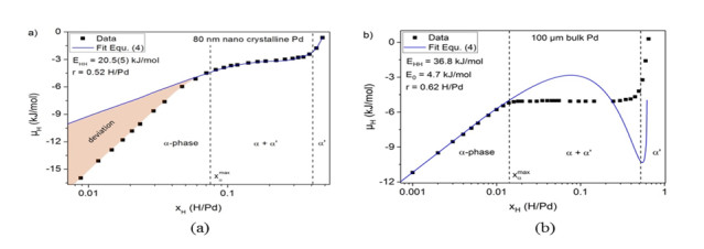
The substrate-induced stress σii can be measured by a substrate deflection method [36,10]. With this measured stress dependency, Eq 4 enables a description of the thermodynamic conditions of hydride formation in the Pd-H thin films adhered to substrates, converging to the measured sloped chemical potential plateau in the two-phase field in terms of a Maxwell-construction—reflecting the measured two-phase co-existence [10,19]. However, as exemplarily shown in Figure 1a for the example of an 80 nm nano crystalline Pd-H film on a silicon substrate, the fit function of Eq 4 (blue line) remarkably deviates from the measured chemical potential in the α-phase region below the solid solution limit. This differs from the measured chemical potential of the Pd-H bulk system (with σii=0) shown in Figure 1b, where the fit function of Eq 4 nicely describes the low concentration regime. We note that deviations of the bulk isotherm from the measured data in the two-phase region of the bulk system in Figure 1b are self-evident: In the concentration range of the two-phase equilibrium, the isotherm oscillates around the measured chemical potential. The constant potential data can be obtained by the Maxwell-construction; this has been targeted in reference [10].
Figure 1.
Chemical potential μH of hydrogen in (a) 80 nm nano crystalline Pd-H adhered to a Si substrate and (b) free standing bulk Pd-H as a function of the hydrogen concentration xH at temperature T = 297 K. Measured data points are given in black dots. The quasi-thermodynamic approach of Eq 4 describes the two-phase (α+α') field in terms of a Maxwell-construction both for bulk and for the thin film, as can be seen by the inserted fit functions given in blue lines. In the solid solution α-phase, Eq 4 clearly deviates from the measured chemical potential for the thin film (a). The phase boundaries were determined by tangent constructions to the measured data points in the logarithmic representation.
Isotherms of Pd thin films of other microstructures and thicknesses are presented in the supplemental information. They show a similar behavior to the film in Figure 1a. Hence, in the manuscript we picture results of the 80 nm nano crystalline Pd film as case examples.
Within the framework of this model, the observed deviation is caused by the restriction to a sole site energy E0 in Eq 4: In thin films a number of microstructural defects such as surfaces, interfaces and dislocations with additional site energies for hydrogen are present. Open-volume defects like grain boundaries, vacancies and the dilatation fields of edge dislocations with a locally expanded lattice can interact attractively with hydrogen induced strain fields and hence offer more negative site energies than the conventional interstitial sites. This results in a preferable H-occupation of open-volume defects [6,18,31]. Re-writing Eq 4 as Eq 5
RTln(xHr−xH)+E0=μH+EHHxH+v0ηHσii(xH)
(5)
illustrates that in case of defective metals the left hand side of the equation has to be replaced by a distribution of sites and site energies [22,31]. Subsequently, we will show that this approach enables a reasonable fit of the measured chemical potential curves of Pd-H thin films in the solid solution regime. Following the approach of an additive contribution of substrate-induced stresses to the chemical potential, the measured stress contribution v0ηHσii(xH) has to be substracted from the measured chemical potential μH to determine pure site energies. Any change in the H-H-interaction contribution EHHxH is neglected, here. It has a minor impact on the isotherm in the low concentration regime, and it would yield a self-referred contribution to the hydrogen concentration xH of the film. Its effect on the fitting parameters in the low concentration regime is discussed in the supplemental information.
Following an approach of Kirchheim et al. [2,22,24,37,38], within the framework of statistical thermodynamics the distribution of hydrogen atoms among a number of different sites can be described by using Fermi-Dirac statistics and the related density of sites (DOS), given by Z(E). Since the chemical potential of hydrogen atoms in different sites is equal at a given overall hydrogen concentration of the film, in turn the total concentration xH of hydrogen atoms in the metal at a given chemical potential μH is determined by integrating over the energies E of Z(E) multiplied with the Fermi-Dirac function (Eq 6) [2,37],
xH(μH)=r⋅∞∫−∞Z(E)1+exp(E−μHRT)dE
(6)
In turn, this enables the reconstruction of the density of sites Z(E), when μH(xH) is measured.
Considering conventional interstitial lattice sites with a sharp site energy E0, the DOS transforms to a delta-distribution (Eq 7) [2],
Z(E)=δ(E−E0)
(7)
In defective metals a fraction f of the interstitial lattice sites is replaced by sites with a different energy distribution. Considering sites like grain boundaries with a distribution of atom arrangements, following an idea of White et al. the DOS can be described by a Gaussian distribution (Eq 8) with half width σ1 around peak energy E1[39,2],
Z(E)=1σ1√π⋅exp(−(E−E1σ1)2)
(8)
For dislocations the situation is more complicated [2,37]. Here, hydrogen atoms tend to form elongated hydrides in the dilatation fields of edge dislocations at low overall hydrogen concentrations in the metal. Considering the related DOS with an energy EV of hydride formation close to the dislocation and assuming an octahedral symmetry of the dislocation sites [2], it is Eq 9 [37]
Z(E)=−ρπ(A⋅VH)22(E−EV)3
(9)
with the dislocation areal density ρ and the partial volume of hydrogen atoms in metals, VH=1.69×10⁻⁶m3/mol[3]. Furthermore, the parameter A is given by A=Gb(1+v)3π(1−v) with shear modulus G=44.7GPa, Burgers vector b=0.275nm and Poisson ratio v=0.523 in the (111) plane of a Pd thin film with [111] texture [10].
To fit the measured chemical potential curves of Pd-H thin films, depending on the film structure we will take into account one or two kinds of sites with sharp site energy E0 and Eil0 (representing interstitial sites) and two different kinds of sites with Gauss distributed site energies E1 and E2. The two Gaussians may represent grain/domain boundary sites and deep traps. As discussed below, we will not consider dislocations. For simplicity, we will furthermore assume r=1H/Pd, neglecting the blocking of octahedral interstitial sites. This is justified at low overall hydrogen concentrations, regarded here. Within our approach we use as few fitting parameters as possible, that can be clearly distinguished from a physical point of view.
In the regular fcc Pd lattice the number of octahedral interstitial sites equals that of the Pd atoms, yielding the relation f0=1−f1−f2 for the number density f0 of available interstitial sites in Pd. For some Pd films (see below), an additional adhesive vanadium interlayer was placed in-between the Pd film and the substrate. This layer offers additional interstitial sites fil0 of site energy Eil0, that add on top of the sites in the Pd film. Then, in total the DOS of the Pd films is given by (Eq 10)
Evaluating the total hydrogen concentration in a film referring to Eq 6, all partial DOS of Eq 10 can be treated separately, and the partial hydrogen concentrations can be summed up, subsequently. Integrating the first two parts of Eq 6 with 10 (Eq 11)
which is equivalent to μH=RTln(xH1−xH)+E0 for f1=f2=fil0=0.
For the Gaussian parts of Eqs 6 and 10 no primitives exist. However, the partial hydrogen concentration xH,1,2 in sites with Gaussian site energy distribution can be calculated numerically, when the integral is transformed into a sum over n discrete energies ∆Ej=(Ej−Ej−1) on a properly chosen energy interval [a,b]. Then (Eq 13),
This sum can be calculated stepwise for discrete values of μH. Together with Eq 12 it yields the total hydrogen concentration as a function of the chemical potential (Eq 14)
xH=xH(μH)
(14)
in the film for each given μH, with E0,Eil0,E1,E2,σ1,σ2,f1 and f2 left as fitting parameters of the DOS to represent the measured chemical potential. fil0, on the other hand, can be calculated from the thickness of the V interlayer. Relative to the Pd layer thickness it is (Eq 15)
fil0=dVdPd⋅vPdvV
(15)
with the thicknesses dV and dPd of the V interlayer and the Pd film, and the molar volumes vV=8.32×10⁻⁶m3/mol of vanadium and vPd=8.56×10⁻⁶m3/mol of palladium [27]. Since we correct the measured chemical potential data for the measured substrate-induced stress contribution, we call our model the “σDOS model”.
The Gaussian functions in Eq 13 decrease rapidly to the left and to the right hand sides of the peak energies. Setting a=−80kJ/mol<Ej≤b=+40kJ/mol and ∆Ej=0.2kJ/mol is a reasonable choice in case of the investigated Pd-H thin films: with the fitting parameters in Table 1, the incremental concentration steps are ∆xjH,1,2<1×10⁻¹⁴ H/Pd at the borders of [a, b].
2.2. Experimental details
24-200 nm Pd films were Ar-ion beam sputtered at 2×10⁻⁴mbar in an UHV chamber with a background pressure of the order of 10−10mbar. The sputter rate was 1nm/min. Microstructure and adhesion conditions of the films were adjusted by choosing two different substrates (Silicon (Si) [001] with its native surface oxide layer and sapphire (Al2O3) [0001]), by choosing the substrate temperature between 300 and 1073 K, and by adding a 1nm adhesive V-interlayer (V//Al2O3) for the epitaxial films. All films contained a small amount of iron xFe=1−2at%, resulting from the film’s cathode beam sputtering in the UHV vessel. The substrates dimensions were 30 mm × 7 mm × (0.1-0.5) mm. The Pd films’ microstructures were described elsewhere [40]. At 300 K, Pd grows with [111] fibre texture and in-plane grain sizes of 30-50 nm on silicon substrates. These films are called “nano crystalline films”. Pd on sapphire sputtered at 673 K has a multi-oriented, polycrystalline microstructure with twinned domains. These films are named “multi-oriented films”. Pd on sapphire with an adhesive V-interlayer grows seeded epitaxially at 673 K. The films are called “epitaxial films”.
After film preparation, XRD stress analysis yields compressive intrinsic in-plane stresses of the order of σ0=−1.3GPa for nano crystalline Pd films on Si. Multi-oriented films on Al2O3 and epitaxial films on V//Al2O3 are strained in tension with stresses of σ0=+0.2to+0.8GPa, see reference [41].
The Pd films were loaded stepwise with hydrogen by electrolytical charging in 2/3 glycerin (80%) and 1/3 phosphoric acid (80%) [19]. The chemical potential μHof hydrogen in the films (Eq 16a) was determined in reference to a saturated Ag/AgCl-electrode, as from Nernst equation [12,13,31]
μH=(U−U0)⋅F+μ0H2(T)/2
(16a)
with Faradays constant F, electromotive force (EMF) U and standard potential U0=0.181V. The standard potential was determined for a 100 µm thick Pd bulk sheet. The offset term in Eq 16a refers to the standard chemical potential of gaseous hydrogen. It is (Eq 16b)
μ0H2/2=−231.8kJ/mol
(16b)
at T=297K, see the supplemental information for details. As conventionally done in the corresponding literature on metal hydrogen systems [2,22,31,37,38,42], we here shift the energy scale by adding −μ0H2/2 to the chemical potential, essentially neglecting the offset term.
H-induced changes ∆σ11≡∆σ of the Pd films’ in-plane stress were determined in-situ by substrate curvature measurement in the long substrate direction. According to Stoney’s equation (Eq 17) [36].
∆σ=ESd2S6(1−vS)df⋅(1R−1R0)
(17)
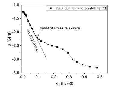
with the substrates’ elastic moduli ES and vS, substrate thickness dS, film thickness df, radius Rof substrate curvature and initial radius R0. The change of the radius of curvature was measured utilizing an induction sensor with a resonant circuit. A metal plate was glued to the backside of the substrates’ front end and placed close to the sensor. When the distance between plate and sensor changes due to substrate-bending, the measured capacity of the sensor changes due to eddy currents induced in the plate. This enables calibration of the substrate curvature [43]. A typical stress-concentration curve is shown in Figure 2 for the exemplary case of the 80 nm nano crystalline Pd-H film. Further stress data of the films was published in references [10] and [41].
Figure 2.
Absolute H-induced modification of the in-plane stress of an 80 nm nano crystalline Pd-H film, as measured in-situ by the substrate deflection method. In the low concentration regime the compressive stress increases almost linear elastically with an increment of −11.3GPa/xH. At xH=0.09(1)H/Pd stress relaxation sets in due to the generation of microstructural defects (mainly dislocations) in the film [41].
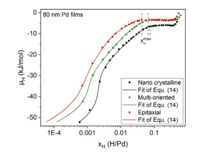
Figure 3 shows the measured, stress-corrected chemical potentials (data points) of 80 nm Pd-H thin films with nano crystalline, multi-oriented and epitaxial microstructures and best fits (lines) according to Eq 14. For the nano crystalline and the multi-oriented film fil0 is fil0=0, while it is fil0=0.0127 for the epitaxial film. Apparently, the measured chemical potentials of the films with different microstructures differ systematically, with the smallest chemical potential at a given H-concentration for the nano crystalline film. This is in accordance with the expectation that nano crystalline films contain the largest number of open-volume defects.
Figure 3.
Measured chemical potentials (data points) of 80 nm Pd-H thin films with different microstructures, each corrected by subtracting the measured substrate-induced stress contribution v0ηHσii(xH) from the measured chemical potentials, compare reference [10]. The data points were fitted (lines) according to Eq 14. The solid solution limit xmaxα of each film is marked.
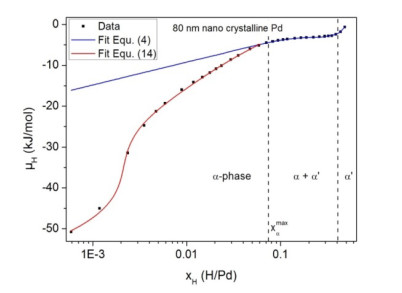
As can be seen, the data points are well represented by the fitted curves. This is also expressed in Figure 4. There, the original, uncorrected μH data of the 80 nm nano crystalline Pd-H thin film is plotted together with the fit according to the quasi-thermodynamic approach of Eq 4 and with the fitted line according to Eq 14. In accordance with the data treatment described before, thereby the measured substrate-induced stress contribution was added back to the curve of Eq 14 after the fitting procedure. While the fit of Eq 4 strongly deviates from the measured chemical potential in the α-phase region, Eq 14 fits well, there. Hence, the fitted DOS with one delta and two Gaussian distributions well represents the measured chemical potential. In the supplemental information, we furthermore show that it is mandatory to use two Gaussian site energy distributions next to the interstitial sites to fit the chemical potential.
Figure 4.
Measured chemical potential of an 80 nm nano crystalline Pd-H thin film with the fitted curves according to the quasi-thermodynamic approach of Eq 4 and the σDOS model according to Eq 14. The substrate-induced stress contribution to the chemical potential was added back to Eq 14 after the fitting procedure. The stress-corrected fit (red curve) describes the data very well in the α-phase region.
The fitted σDOS model parameters of Eq 14 are summarized in Table 1 for all investigated Pd-H films. Related isotherms are presented in the supplemental information. Reference data for bulk Pd according to references [10,22,32] is given in Table 1, as well. The fits are very sensitive to small changes in the fit parameters, yielding considerably small confidence intervals. This is discussed in more detail in the supplemental information.
Table 1.
Parameters of the fitted DOS of Pd-H thin films with different microstructures according to Eq 14. Three kinds of sites with sharp site energy E0 and two Gaussian site energy distributions with E1,2, half widths σ1,2 and site fractions f1,2 are distinguished for the nano crystalline and the multi-oriented Pd films, while additional sites with energy Eil0 were considered for the epitaxial Pd films with a 1 nm V interlayer. In the right column the number ratio NS/NV of surface-to-volume Pd atoms of the films is given. For comparison, reference data for bulk Pd [10,22,32] is quoted. The nano crystalline bulk samples were prepared by compacting inert gas condensated (IGC) nano particles [22]. To calculate NS/NV for bulk, samples of 80μm thickness like in reference [22] were assumed.
Thickness (nm)
E0 (kJ/mol)
Eil0 (kJ/mol)
E1 (kJ/mol)
σ1 (kJ/mol)
f1
E2 (kJ/mol)
σ2 (kJ/mol)
f2
NSNV
Epitaxial Pd on 1 nm V/Al2O3 [0001], TDep = 673 K
24
4.6(3)
-0.8(5)
0.6(1)
17.9(3)
0.070(2)
-43(1)
11.3(3)
0.0019(1)
0.0091
80
5.7(3)
-0.3(9)
0.6(1)
19.3(3)
0.019(2)
-43(1)
8.1(3)
0.0007(1)
0.0027
200
4.8(3)
-0.3(9)
0.5(1)
17.1(5)
0.017(2)
-42(1)
8.1(3)
0.0002(1)
0.0011
Multi-oriented Pd on Al2O3 [0001], TDep = 673 K
24
1.8(3)
n/a
0.5(1)
15.3(3)
0.124(2)
-46(1)
9.4(3)
0.003(1)
0.0091
80
4.4(3)
n/a
0.5(1)
16.6(3)
0.055(2)
-45(1)
5.6(3)
0.0013(1)
0.0027
200
4.5(3)
n/a
0.5(1)
17.4(3)
0.032(2)
-42(1)
8.1(3)
0.0005(1)
0.0011
Nano crystalline Pd on Si [100], TDep = 300 K
24
1.0(3)
n/a
0.5(1)
14.5(3)
0.25(2)
-44.0(5)
5.9(3)
0.003(1)
0.0091
80
1.5(3)
n/a
0.5(1)
15.0(3)
0.118(2)
-48.3(5)
6.3(3)
0.0021(1)
0.0027
200
1.0(3)
n/a
0.7(1)
14.5(3)
0.100(2)
-48.0(5)
7.1(3)
0.0015(1)
0.0011
Reference: coarse grained [10,32] and nano crystalline [22] bulk Pd
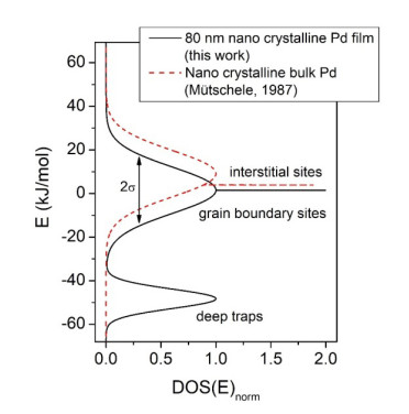
In Figure 5, the fitted density of sites of the 80 nm nano crystalline Pd-H film is compared to the DOS determined by Mütschele and Kirchheim for nano crystalline bulk in reference [22].
Figure 5.
Normalized density of sites (DOS) determined with the σDOS model for an 80 nm nano crystalline Pd-H film, compared to the DOS of nano crystalline bulk Pd-H [22]. The plotted DOS were normalized to peak heights of 1 to enhance the comparability.
Figure 4 exemplarily shows the measured data for one chosen Pd-H film, and two related fit curves of the quasi-thermodynamic approach and the σDOS model. For both fit curves, the measured stress contribution to the chemical potential is separated from the fitting procedure. The quasi-thermodynamic approach (blue line) considers octahedral interstitial sites only, which hydrogen occupies in bulk material. The red line according to the fitted DOS in Figure 5 touches the curve of the quasi-thermodynamic approach close to the solid solution limitxmaxα of the film. This observation hints on saturation of sites different from octahedral interstitial sites within the films’ α-phase region. Furthermore, it shows that the onset of hydride formation in the films is determined by hydrogen located in interstitial sites.
On a closer look the slope of the σDOS model curve is larger than that of the quasi-thermodynamic approach close to xmaxα. This effect is caused by the H-H interaction not implemented in Eq 14, that bends down μH(xH) when the film enters the plateau region of the two-phase field [10,22]. This aspect is discussed in the supplemental information.
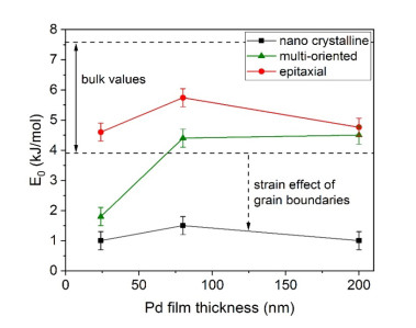
The absolute values of E0 of the interstitial sites in Pd are plotted in Figure 6 together with the marked range (between the dashed lines) of bulk values [10,22,32] for the energy range determined for octahedral interstitial sites in Pd.
Figure 6.
Octahedral site energies E0 determined for Pd-H thin films of different microstructures, compared to the range of literature data of the respective bulk values for Pd-H. The site energies of the nano crystalline films are presumably reduced by a strain effect of the grain boundaries acting on the grains [23,44].
Apparently, the site energy values E0 of the thicker multi-oriented (green triangles) and of the epitaxial (red spheres) Pd-H films fall into the range of the bulk values, while that of the nano crystalline films (black squares) and of the thinnest 24 nm multi-oriented film are reduced by 2−3kJ/mol. This hints on an interfacial stress contribution of the grain boundaries on the grains, as proposed by Weissmüller and Lemier [23,44]: In their model, the hydrogen filled grain boundaries affect the grain interior of nano crystalline Pd-H samples. In the low concentration α-phase regime the H-occupation of grain boundary sites leads to a tensile straining of the grain interior, which increases the H binding energy to the interstitial sites, expressed by a reduction of the site energy E0.
In thin films adhered to rigid substrates, all straining effects are anisotropic, yielding a surplus vertical expansion and hence a tetragonal distortion of the films [41]. Hence, the grain-boundary straining effect will be anisotropic, as well, and it should increase with an increasing volume fraction of grain boundaries. This is confirmed by the fitting parameters in Table 1.
According to Table 1, for all investigated Pd-H thin films the obtained grain boundary energies E1 and the half widths σ1 of the energy distributions are similar within E1=0.5−0.7kJ/mol and σ1=15−19kJ/mol, respectively. This remarkable result is not expected at first hand, since the grain boundary structure of nano crystalline films and of films of other microstructures can be assumed to differ. However, it has been shown both for fibre textured as well as for epitaxial metal thin films that the crystalline texture assists the formation of special low-Σ grain boundary fractions [45,46,47], forming a two dimensional network with general grain boundary fractions [45,48]. This supports the experimental result that grain/domain boundaries in Pd-H thin films of different microstructures can be described by similar model parameters. Interestingly, the half widths σ1 of the site energy distributions are also similar to the bulk value of 15kJ/mol determined for nano crystalline Pd in reference [22]. But, the absolute grain boundary energy E1 is shifted to less positive values for the thin films compared to the value of 9.1kJ/mol for Mütscheles and Kirchheims nano crystalline bulk Pd [22]. Hence, hydrogen is bound more strongly to grain/domain boundary sites in thin films compared to their nano crystalline bulk Pd samples. This observation suggests that the grain boundary structure of sputtered thin films differs from that of these nano crystalline bulk samples. This may result from the different preparation process of compacting gas phase condensated nano particles, the consolidating inert gas condensation (IGC) method [22,49]. As shown in Refs. [49,50], IGC nano crystalline bulk Pd samples similar to those investigated in reference [22] contain light element impurities (O, N, H) by preparation. The impurity content linearly increases with an increasing surface-to-volume ratio of the particles. This indicates that the impurities segregate to the grain boundaries of the samples, where they can block absorption sites for further hydrogen occupation. This might increase the mean grain boundary energy E1 of nano crystalline bulk Pd. At a particle size of 5−10nm like in reference [22], a total impurity content of 4.5−9at% is expected [50], with atom ratios O:H:N of 6:4:3 [49]. Complementary, possible segregation of substrate material, i.e. Si or V, in the grain/domain boundaries of the sputtered Pd films would change the film’s site energies compared to bulk material. Gemma et al. have investigated the interdiffusion of V and Pd by means of atom probe tomography, resulting in a steady V content of the order of 5at% in Pd close to the interface [51].
Another cause of reduced grain/domain boundary energies in thin films might be related to structural changes due the tetragonal distortion of adhered thin films, like it is observed for the interstitial site energies, as well.
Furthermore, for nano crystalline bulk Pd consisting of randomly oriented nano particles, grain boundaries with a partially amorphous intergranular phase have been reported [17,49,52]. Consideration of the similar widths σ1 of the energy distributions suggests that the general grain boundary fraction of the thin films contains amorphous parts, as well.
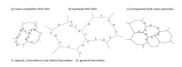
The grain/domain boundary structures proposed for nano crystalline and epitaxial Pd thin films as well as for nano crystalline bulk Pd are schematically compared in Figure 7.
Figure 7.
Proposed grain/domain boundary structure of (a) nano crystalline and (b) epitaxial Pd thin films viewing onto the film surface, and (c) of nano crystalline bulk Pd, consistent with the experimental findings applying the σDOS model to Pd-H. We interpret our results for the thin films with grain/domain boundaries containing special, coincidence site lattice boundary fractions (S boundaries) and general, large angle boundaries (G boundaries). These form a two dimensionally alternating network. The nano crystalline bulk sample, prepared by compacting randomly oriented nano particles, mainly should contain general grain boundaries with a certain fraction of surplus atoms of O, H and N. In all cases the general boundaries seem to contain amorphous parts.
Next to grain/domain boundary sites, deep traps are found for the Pd-H thin films. Their energy values E2 range between E2=−42kJ/mol and E2=−48kJ/mol. However, they group for the different microstructures with more positive values for the epitaxial films and more negative values for the nano crystalline films. Regarding the nature of these deep traps, three constituents of the films’ microstructure are at hand: the films’ surface, a natural surface oxide layer, and vacancies. Additionally, for the case of epitaxial Pd thin films the thin vanadium interlayer acts as a hydrogen trap, see Table 1. This was expected, since the binding energy of H to vanadium is larger than that to palladium [27,51]. In the present study, the chemical potential of the Pd thin films’ surface oxide layer was determined by anodic polarization of the films in the electrolyte, see the supplemental information for details. It ranges between −45and −80kJ/mol, depending on the degree of oxidation. Hence, the measured deep trap energies fall into the range of Pd oxide potentials. Furthermore, literature data for the adsorption energy of hydrogen atoms on clean Pd(111) surfaces are of a similar order of magnitude. Ferrin et al. and Dong et al. calculated H trapping energies of −46kJ/mol[53] (the values therein were corrected by −μ0H2/2) to −49kJ/mol[54] on Pd(111) surfaces. Conrad and Ertl et al. measured −44kJ/mol[55]. All of these energy values indicate the presence of deep traps at the Pd-H films surfaces. Additionally, hydrogen can be trapped in vacancies in the bulk of the films [18]. The trapping energy of Pd vacancies decorated with H-atoms changes with the number of trapped H. According to reference [56] the trapping energy is −22kJ/mol for one H atom, −45kJ/mol for two H atoms, and it decreases down to −112kJ/mol for six trapped H atoms. With this, it is improbable that vacancies widely contribute to hydrogen trapping in the investigated Pd-H thin films, since their filling should not saturate at two hydrogen atoms.
To evaluate the nature of the deep traps in more detail, the site fractions f2 given in Table 1 are compared to the number density of surface sites of Pd thin films. Owing to the Burgers vector b=0.275nm, the (111) surface plane of the Pd thin films consists of NS=2.54×10⁻⁹mol/cm2 Pd atoms. With the molar volume vPd=8.56×10⁻⁶m3/mol[27] of Pd, a 1cm2 film of 80nm thickness consists of NV=9.35×10⁻⁷mol Pd atoms in total. Hence, for this film NS/NV=0.0027. Surface atom fractions NS/NV of films with other thicknesses are listed in the last column of Table 1. Assuming that at maximum 1 H atom is adsorbed per Pd surface atom [55], NS/NV represents the maximum surface site fraction of H atoms on the films.
For all investigated films apart from 200nmnano crystalline Pd-H, Table 1 reveals f2<NS/NV. Thus, hydrogen adsorption to surface sites can explain the experimental findings. However, for most films a certain amount of surface sites seems to be blocked for hydrogen adsorption. For other surface sites, the natural surface oxide will be reduced by the formation of water molecules, which are dissolved in the electrolyte and open surface trap sites for H atoms. Thereby, the loss of hydrogen atoms by water formation in the electrochemical loading experiments results in an apparent lowering of the chemical potential in the plots of μH(xH) in Figures 3 and 4. The related effect will be three times that of direct H trapping on the Pd surface: Two hydrogen atoms bind to one surface oxygen atom, and a further hydrogen atom binds to the nascent surface site after dissolution of the generated water molecule. According to the values of f2, hydrogen trapping in vacancies, again, is of minor importance in the measured Pd-H thin film isotherms.
One can estimate the volume fraction v1 of grain/domain boundary sites in the Pd films, when the site fractions f1 are identified with the defects’ volume fraction in the metal [22,37]. This implies that each defect site has the partial volume v0 of an octahedral interstitial site, compare Eq 10. This is analogous to an attempt of Löffler et al. [49], who successfully described the contribution of disordered grain boundaries to X-ray scattering intensities of nano crystalline bulk Pd, assuming that the atom density of disordered grain boundaries matches that of the crystal lattice.
Nano crystalline thin films often consist of columnar grains, ranging from the top close to the bottom of the film [57]. The multi-oriented and the epitaxial Pd films investigated in this study consist of large domains [41,58], that can be described as columns, as well. Assuming columnar grains/domains with diameter D and grain/domain boundaries of width ∆, the grain boundary volume fraction is given as (Eq 18)
f1=v1=1−(DD+∆)2
(18)
With the established value of ∆=0.9nm for grain boundaries in nano crystalline bulk Pd [2,59] according mean grain/domain sizes were calculated and are listed in the left column of Table 2 for the different Pd-H films.
Table 2.
Lateral grain/domain sizes D calculated from the site fractions f1 of domain boundary sites, assuming a domain boundary width of ∆=0.9nm and O- or T-site occupation by hydrogen atoms in the domain boundaries (GB).
The resulting grain/domains sizes are of a reasonable order of magnitude, but they are systematically too small compared to measured lateral grain/domain sizes of the films as determined by SEM. For the example of the 200nm nano crystalline Pd film a lateral grain size of 30−50nm was measured [41,57,58]. But, the domains were measured to span more than 100nm in the multi-oriented films and several hundred nm in the epitaxial films [41,57,58].
Considering this observation, different explanations are at hand. (ⅰ) first, the defect volume fractions might be over-estimated by Eq 14, if a significant kind of defect was neglected in Eq 10, for example dislocations. Another possible explanation might be linked to the assumption underlying Eq 18, e.g. that (ⅱ) the partial volume of grain boundary sites equals that of octahedral interstitial sites. Finally, (ⅲ) the adapted bulk grain boundary width ∆ might be too small for the thin films. These aspects are discussed subsequently.
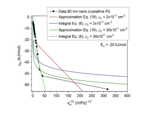
To determine (ⅰ) the dislocation effect on the chemical potential of metal-hydrogen systems, the respective DOS of Eq 9 needs to be introduced into Eq 6. With a step-function approximation of the site occupancy, Kirchheim has shown that Eq 6 then yields the chemical potential contribution (Eq 19) [37].
μVH=EV−A⋅VH2(rρπxV)1/2
(19)
with the hydrogen concentration xV of dislocations.
If xV is not small, Eqs 6 with 9 needs to be integrated numerically. Both results are shown in Figure 8 for differently assumed dislocation densities ρ and compared to the data of the 80 nm nano crystalline Pd-H film. The hydride formation energy of the dislocations was set to EV=−20kJ/mol[37]. The dislocation densities were set to ρ=2×1011cm−2, which is typical for strongly deformed metals, and (for the plot) to ρ=30×1011cm−2.
Figure 8.
Comparison of the measured chemical potential of an 80 nm nano crystalline Pd-H film with the expected contributions of dislocations with different dislocation areal densities ρ according to Eqs 6 and 19, respectively.
Figure 8 shows that the film data are not represented by the curves for reasonable dislocation densities. An un-physically high dislocation density would be needed to approach the data. The reason is that the measured chemical potential of hydrogen in the Pd films increases much slower with the film’s hydrogen concentration than predicted by a primary dislocation effect, see the supplemental information. Hence, in the chemical potential of the solid solution regime of Pd-H thin films dislocations do not play a major role, and they can be neglected in the DOS evaluation.
Assuming the site fractions f1 to be correct, (ⅱ) a possibility to explain too small calculated grain/domain sizes D can be found in the geometry of the grain/domain boundary sites. Boundary sites with different character than octahedral (O)-sites might be occupied—such as tetrahedral (T)-sites. In the fcc lattice two T-sites exist per metal atom, while there is only one O-site per atom [3]. The DOS in Eq 10, however, represents the numbers fOi of sites replacing O-sites. Hence, assuming T-boundary sites, Eq 10 needs to be re-written (Eq 20):
with fT1=2⋅fO1˙=f1 in Table 1. We note that in principle only 50% of these T-sites (according to a maximum concentration of 1H/Pd) can be occupied by H atoms, since the nearest neighbour distance of the T-sites is 1.95 Å or 2.75 Å in the unit cell of palladium, respectively. The value of 1.95 Å is slightly smaller than Switendicks criterion for the minimum distance of 2.1 Å for neighbouring H atoms in the metal lattice due to a short ranged, repulsive electronic H-H interaction [59]. However, with a certain degree of disorder in the general grain/domain boundary fractions of the Pd thin films, one can assume that the positions of the T-sites are slightly distorted, making more T-sites available for hydrogen. Furthermore, in general it is not expected that the grain boundary sites are entirely occupied by H atoms, since the grain boundaries do not undergo hydride formation [22].
Since f1 is small, the consideration of T-sites does not significantly change the fitting parameters in Table 1. In case of the 80 nm nano crystalline Pd film E0 is reduced by 0.2kJ/mol, while the other fitting parameters remain constant. For most other films f1 is even smaller, yielding smaller corrections.
But, the change of the type of grain/domain boundary sites changes the volume density of domain boundaries in Eq 18, since (Eq 21)
v1=fO1=fT12=f12
(21)
yields (Eq 22)
fT1=2−2(DD+∆)2
(22)
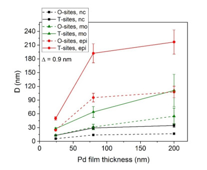
for T-sites, when no restrictions apply for the T-site occupancy. Since ∆≪D, this scales up the lateral domain diameters D approximately by a factor of 2. The resulting domain sizes are listed in the right column of Table 2, as well. All domain sizes are plotted as a function of film thickness in Figure 9.
Figure 9.
Calculated lateral domain sizes for Pd thin films with nano crystalline (nc), multi-oriented (mo) and epitaxial (epi) microstructures, consisting of columnar domains and O- or T-domain boundary sites. A grain/domain boundary width of ∆=0.9nm was assumed [2,60]. The comparison with measured domain sizes suggests a preferred T-site occupancy of hydrogen in the domain boundaries.
ⅲ) The third explanation could be a different grain boundary width ∆. According to Eq 22, the calculated grain/domain size D scales linearly with the geometrical boundary width ∆ (Eq 23),
D=∆⋅√2−fT1√2−√2−fT1
(23)
Hence, the grain/domain sizes would scale up, if the grain/domain boundary width ∆ were larger than expected. This might be interpreted by a certain underestimation of the grain boundary width ∆ for the nano crystalline bulk Pd in reference [22], taking the possible fraction of surplus atoms into account, that may block sites for hydrogen occupation at the grain boundaries. If this assumption were correct, the enhanced open-volume of the grain/domain boundaries of the thin films would deliver further arguments for a lowered site energy of grain/domain sites of Pd-H thin films compared to the nano crystalline bulk Pd-H grain boundaries.
In total, the fitted DOS and the resulting domain sizes suggest that H atoms are occupying T-sites in the domain boundaries of Pd thin films rather than O-sites. This suggestion matches the observed site occupancy in amorphous metals [14,38,42]. It fits to the proposition of partly amorphous intergranular phase fractions in the nano crystalline bulk as well as the Pd-H thin films. Additionally, the grain boundary width seems to be slightly larger than 0.9 nm.
5.
Conclusions
The site energy distribution in Pd-H thin films can be successfully described by the proposed σDOS model which considers the substrate-induced stress impact as well as interstitial sites, grain boundary sites and deep trap sites for hydrogen. Within this σDOS model we can reveal information about the films’ microstructure.
This model is not restricted to Pd-H thin films, but it will be applicable to a variety of systems, where substrate-induced stresses and microstructural constituents significantly contribute to the site occupancy of solute atoms, that segregate to open-volume defects. This pure thermodynamic approach can supplement the microstructural analysis of alloy systems by other quantitative techniques, such as positron annihilation spectroscopy, neutron diffraction or transmission electron microscopy. This will be of high interest in the investigation of thin film metal-hydrogen systems containing special microstructural constituents of high content. Other examples are light elements such as carbon, nitrogen, oxygen or lithium in metals, but segregating metallic alloys such as bismuth in copper, as well.
Acknowledgements
Financial support of the Deutsche Forschungsgemeinschaft (DFG) via Projects PU131/7-2, PU131/9-1 and PU131/12-1 is gratefully acknowledged.
Conflict of interests
The authors declare no conflicts of interest in this paper.
References
[1]
Peisl H (1978) Lattice strains due to hydrogen in metals, In: Alefeld G, Völkl J, Hydrogen in Metals I-Basic Properties, Heidelberg: Springer-Verlag.
[2]
Kirchheim R, Pundt A (2015) Hydrogen in Metals, In: Laughlin D, Hono K, Physical Metallurgy, 5 Eds., Elsevier, 2597-2705.
[3]
Fukai Y (2005) The Metal-Hydrogen System: Basic Bulk Properties, Heidelberg: Springer-Verlag.
[4]
Mooij L, Perkisas T, Palsson G, et al. (2014) The effect of microstructure on the hydrogenation of Mg/Fe thin film multilayers. Int J Hydrogen Energ 39:17092-17103. doi: 10.1016/j.ijhydene.2014.08.035
[5]
Hjörvarsson B, Andersson G, Karlsson E (1997) Metallic superlattices: Quasi two-dimensional playground for hydrogen. J Alloy Compd 253:51-57.
Gremaud R, Gonzales-Silveira M, Pivak Y, et al. (2009) Hydrogenography of PdHx thin films: Influence of H-induced stress relaxation processes. Acta Mater 57:1209-1219. doi: 10.1016/j.actamat.2008.11.016
[8]
Baldi A, Gonzales-Silveira M, Palmisano V, et al. (2009) Destabilization of the Mg-H system through elastic constraints. Phys Rev Lett 102: 226102. doi: 10.1103/PhysRevLett.102.226102
[9]
Griessen R, Strohfeldt N, Giessen H (2016) Thermodynamics of the hybrid interaction of hydrogen with palladium nanoparticles. Nat Mater 15: 311-317. doi: 10.1038/nmat4480
[10]
Wagner S, Pundt A (2016) Quasi-thermodynamic model on hydride formation in palladium-hydrogen thin films: Impact of elastic and microstructural constraints. Int J Hydrogen Energ 41: 2727-2738. doi: 10.1016/j.ijhydene.2015.11.063
[11]
Schwarz R, Khachaturyan A (2006) Thermodynamics of open two-phase systems with coherent interfaces: Application to metal-hydrogen systems. Acta Mater 54: 313-323. doi: 10.1016/j.actamat.2005.08.044
[12]
Boes N, Züchner H (1976) Electrochemical methods for studying diffusion permeation and solubility of hydrogen in metals. J Less Common Met 49: 223-240. doi: 10.1016/0022-5088(76)90037-0
[13]
Züchner H, Rauf T (1991) Electrochemical isotherm measurements on the Pd-H and PdAg-H systems. J Less Common Met 172-174: 816-823. doi: 10.1016/0022-5088(91)90208-L
[14]
Samwer K, Johnson W (1983) Structure of glassy early-transition-late-transition-metal hydrides. Phys Rev B 28: 2907-2913. doi: 10.1103/PhysRevB.28.2907
[15]
Myers S, Baskes M, Birnbaum H, et al. (1992) Hydrogen interaction with defects in crystalline solids. Rev Mod Phys 64: 559-617. doi: 10.1103/RevModPhys.64.559
[16]
Baldi A, Narayan T, Koh A, et al. (2014) In situ detection of hydrogen induced phase transitions in individual palladium nanocrystals. Nat Mater 13: 1143-1148. doi: 10.1038/nmat4086
[17]
Iwaoka H, Arita M, Horita Z (2016) Hydrogen diffusion in ultrafine-grained palladium: Roles of dislocations and grain boundaries. Acta Mater 107: 168-177. doi: 10.1016/j.actamat.2016.01.069
[18]
Melikhova O, Cizek, J, Prochazka I (2014) Hydrogen induced defects in palladium. Acta Phys Pol A 125: 752-755. doi: 10.12693/APhysPolA.125.752
[19]
Wagner S, Klose P, Burlaka V, et al. (2019) Structural phase transitions in niobium hydrogen thin films: Mechanical stress, phase equilibria and critical temperatures. ChemPhysChem 20: 1890-1904. doi: 10.1002/cphc.201900247
[20]
Mooji L, Dam B (2013) Hysteresis and the role of nucleation and growth in the hydrogenation of Mg nanolayers. Phys Chem Chem Phys 15: 2782-2792. doi: 10.1039/c3cp44441d
[21]
Uchida H, Wagner S, Hamm M, et al. (2015) Absorption kinetics and hydride formation in magnesium films: Effect of driving force revisited. Acta Mater 85: 279-289. doi: 10.1016/j.actamat.2014.11.031
[22]
Mütschele T, Kirchheim R (1987) Segregation and diffusion of hydrogen in grain boundaries of palladium. Scripta Metall 21: 135-140. doi: 10.1016/0036-9748(87)90423-6
[23]
Weissmüller J, Lemier C (1999) Lattice constants of solid solution microstructures: The case of nanocrystalline Pd-H. Phys Rev Lett 82: 213-216. doi: 10.1103/PhysRevLett.82.213
[24]
Song G, Geitz M, Abromeit A, et al. (1996) Solubility isotherms of hydrogen in epitaxial Nb(110) films. Phys Rev B 54:14093-14101. doi: 10.1103/PhysRevB.54.14093
[25]
Hamm M, Burlaka V, Wagner S, et al. (2015) Achieving reversibility of ultra-high mechanical stress by hydrogen loading of thin films. Appl Phys Lett 106: 243108. doi: 10.1063/1.4922285
[26]
Laudahn U, Pundt A, Bicker M, et al. (1999) Hydrogen-induced stress in Nb single layers. J Alloy Compd 293-295: 490-494. doi: 10.1016/S0925-8388(99)00471-5
[27]
Wicke E, Brodowsky H (1978) Hydrogen in palladium and palladium alloys, In: Alefeld G, Völkl J, Hydrogen in Metals II, Berlin, Heidelberg: Springer-Verlag.
[28]
Lacher J (1937) A theoretical formula for the solubility of hydrogen in palladium. P Roy Soc Lond A-Mat 161: 525-545. doi: 10.1098/rspa.1937.0160
[29]
Olsson S, Blixt A, Hjörvarsson B (2005) Mean-field-like structural phase transition of H in Fe/V(001) superlattices. J Phys-Condens Mat 17: 2073-2084. doi: 10.1088/0953-8984/17/13/007
[30]
Papaconstantopoulos D, Klein B, Economou E, et al. (1978) Band structure and superconductivity of PdDx and PdHx. Phys Rev B 17: 141-150.
[31]
Kirchheim R (1988) Hydrogen solubility and diffusivity in defective and amorphous metals. Prog Mater Sci 32: 261-325. doi: 10.1016/0079-6425(88)90010-2
[32]
Züttel A (1988) Metall-hydride. Vorlesungsskript.
[33]
Larché F, Cahn J (1973) A linear theory of thermochemical equilibrium of solids under stress. Acta Metall 21: 1051-1063. doi: 10.1016/0001-6160(73)90021-7
[34]
Larché F, Cahn J (1985) The interactions of composition and stress in crystalline solids. Acta Metall 33: 331-357. doi: 10.1016/0001-6160(85)90077-X
[35]
Wagner S, Moser M, Greubel C, et al. (2013) Hydrogen microscopy-Hydrogen distribution in buckled niobium hydrogen thin films. Int J Hydrogen Energ 38: 13822-13830. doi: 10.1016/j.ijhydene.2013.08.006
[36]
Ohring M (1992) The materials science of thin films, San Diego: Academic Press.
[37]
Kirchheim R (1981) Interaction of hydrogen with dislocations in palladium-II. Interpretation of activity results by a Fermi-Dirac distribution. Acta Metall 29: 845-853.
[38]
Bankmann J, Pundt A, Kirchheim R (2003) Hydrogen loading behaviour of multi-component amorphous alloys: model and experiment. J Alloy Compd 356: 566-569.
[39]
White C, Stein D (1978) Sulfur segregation to grain boundaries in Ni3Al and Ni3(Al, Ti) alloys. Metall Trans A 9: 13-22. doi: 10.1007/BF02647165
[40]
Wagner S, Pundt A (2011) Combined impact of micro-structure and mechanical stress on the electrical resistivity of PdHc thin films. Acta Mater 59: 1862-1870. doi: 10.1016/j.actamat.2010.11.052
[41]
Wagner S, Kramer T, Uchida U, et al. (2016) Mechanical stress and stress release channels in 10-350 nm palladium hydrogen thin films with different micro-structures. Acta Mater 114: 116-125. doi: 10.1016/j.actamat.2016.05.023
[42]
Kirchheim R, Mütschele T, Kieninger W (1988) Hydrogen in amorphous and nanocrystalline metals. Mater Sci Eng 99: 457-462. doi: 10.1016/0025-5416(88)90377-1
[43]
Pundt A, Nikitin E, Pekarski P, et al. (2004) Adhesion energy between metal films and polymers obtained by studying buckling induced by hydrogen. Acta Mater 52: 1579-1587. doi: 10.1016/j.actamat.2003.12.003
[44]
Lemier C, Weissmüller J (2007) Grain boundary segregation, stress and stretch: effects on hydrogen absorption in nanocrystalline palladium. Acta Mater 55: 1241-1254. doi: 10.1016/j.actamat.2006.09.030
[45]
Tan L, Allen T, Busby J (2013) Grain boundary engineering for structure materials of nuclear reactors. J Nucl Mat 441: 661-666. doi: 10.1016/j.jnucmat.2013.03.050
[46]
Chan S (1994) Degenerate epitaxy, coincidence epitaxy and origin of "special" boundaries in thin films. J Phys Chem Solids 55: 1137-1145. doi: 10.1016/0022-3697(94)90131-7
[47]
Brons J, Thompson G (2013) A comparison of grain boundary evolution during grain growth in fcc metals. Acta Mater 61:3936-3944. doi: 10.1016/j.actamat.2013.02.057
[48]
Divakar R, Raghunathan V (2003) Characterisation of interfaces in nanocrystalline palladium. Sadhana 28: 47-62. doi: 10.1007/BF02717125
[49]
Löffler J, Weissmüller J (1995) Grain-boundary atomic structure in nanocrystalline palladium from x-ray atomic distribution functions. Phys Rev B 52: 7076-7093. doi: 10.1103/PhysRevB.52.7076
[50]
Haas V, Birringer R, Gleiter H (1998) Preparation and characterisation of compacts from nanostructured powder produced in an aerosol flow condenser. Mater Sci Eng A-Struct 246: 86-92. doi: 10.1016/S0921-5093(97)00754-5
[51]
Gemma R (2011) Hydrogen in V-Fe thin films and Fe/V-Fe multi-layered thin films [Dissertation]. Göttingen: University of Gottingen.
[52]
Keblinski P, Wolf D, Phillpot S, et al. (1999) Structure of grain boundaries in nanocrystalline palladium by molecular dynamics simulation. Scripta Mater 41: 631-636. doi: 10.1016/S1359-6462(99)00142-6
[53]
Ferrin P, Kandoi S, Nilekar A, et al. (2012) Hydrogen adsorption, absorption and diffusion on and in transition metal surfaces: A DFT study. Surf Sci 606: 679-689. doi: 10.1016/j.susc.2011.12.017
[54]
Dong W, Ledentu V, Sautet Ph, et al. (1998) Hydrogen adsorption on palladium: a comparative theoretical study of different surfaces. Surf Sci 411: 123-136. doi: 10.1016/S0039-6028(98)00354-9
[55]
Conrad H, Ertl G, Latta E (1974) Adsorption of hydrogen on palladium single crystal surfaces. Surf Sci 41: 435-446. doi: 10.1016/0039-6028(74)90060-0
[56]
Vekilova O, Bazhanov D, Simak S, et al. (2009) First-principles study of vacancy-hydrogen interaction in Pd. Phys Rev B 80: 024101.
[57]
Cizek J, Melikhova O, Vlcek M, et al. (2014) Hydrogen interaction with defects in nanocrystalline, polycrystalline and epitaxial Pd films. J Nano Res 26: 123-133.
[58]
Wagner S (2014) Dünne palladium-wassersoff-schichten als modellsystem [Dissertation]. Göttingen: University of Göttingen.
[59]
Switendick A (1979) Band structure calculations for metal hydrogen systems. Z Phys Chem 117: 89-112. doi: 10.1524/zpch.1979.117.117.089
[60]
Weissmüller J, Lemier C (2000) On the size dependence of the critical point of nanoscale interstitial solid solutions. Phil Mag Lett 80: 411-418.
Jens Möllmer, Hans Uhlig, Marcus Lange, Jörg Hofmann, Andrei L. Kolesnikov, Yury A. Budkov, André Götze, Holger Kohlmann,
Thermodynamics of hydrogen sorption in MgPd2,
2021,
859,
09258388,
157782,
10.1016/j.jallcom.2020.157782
2.
Wang Liu, Yann Magnin, Daniel Förster, Julie Bourgon, Thomas Len, Franck Morfin, Laurent Piccolo, Hakim Amara, Claudia Zlotea,
Size-dependent hydrogen trapping in palladium nanoparticles,
2021,
2050-7488,
10.1039/D0TA12174F
3.
Raju Lipin, Apinya Ngoipala, Ryan Lacdao Arevalo, Matthias Vandichel,
Computational surface Pourbaix diagrams to unravel cathodic hydride formation on defective palladium surfaces,
2024,
61,
03603199,
460,
10.1016/j.ijhydene.2024.02.248
4.
Astrid Pundt, Stefan Wagner,
Hydrogen Interactions with Defects in Materials,
2024,
96,
0009-286X,
182,
10.1002/cite.202300235
5.
Svetlana Korneychuk, Stefan Wagner, Darius Rohleder, Philipp Vana, Astrid Pundt,
Local Hydrogen Concentration and Distribution in Pd Nanoparticles: An In Situ STEM‐EELS Approach,
2024,
1613-6810,
10.1002/smll.202407092
Stefan Wagner, Astrid Pundt. Hydrogen as a probe for defects in materials: Isotherms and related microstructures of palladium-hydrogen thin films[J]. AIMS Materials Science, 2020, 7(4): 399-419. doi: 10.3934/matersci.2020.4.399
Stefan Wagner, Astrid Pundt. Hydrogen as a probe for defects in materials: Isotherms and related microstructures of palladium-hydrogen thin films[J]. AIMS Materials Science, 2020, 7(4): 399-419. doi: 10.3934/matersci.2020.4.399
Table 1.
Parameters of the fitted DOS of Pd-H thin films with different microstructures according to Eq 14. Three kinds of sites with sharp site energy E0 and two Gaussian site energy distributions with E1,2, half widths σ1,2 and site fractions f1,2 are distinguished for the nano crystalline and the multi-oriented Pd films, while additional sites with energy Eil0 were considered for the epitaxial Pd films with a 1 nm V interlayer. In the right column the number ratio NS/NV of surface-to-volume Pd atoms of the films is given. For comparison, reference data for bulk Pd [10,22,32] is quoted. The nano crystalline bulk samples were prepared by compacting inert gas condensated (IGC) nano particles [22]. To calculate NS/NV for bulk, samples of 80μm thickness like in reference [22] were assumed.
Thickness (nm)
E0 (kJ/mol)
Eil0 (kJ/mol)
E1 (kJ/mol)
σ1 (kJ/mol)
f1
E2 (kJ/mol)
σ2 (kJ/mol)
f2
NSNV
Epitaxial Pd on 1 nm V/Al2O3 [0001], TDep = 673 K
24
4.6(3)
-0.8(5)
0.6(1)
17.9(3)
0.070(2)
-43(1)
11.3(3)
0.0019(1)
0.0091
80
5.7(3)
-0.3(9)
0.6(1)
19.3(3)
0.019(2)
-43(1)
8.1(3)
0.0007(1)
0.0027
200
4.8(3)
-0.3(9)
0.5(1)
17.1(5)
0.017(2)
-42(1)
8.1(3)
0.0002(1)
0.0011
Multi-oriented Pd on Al2O3 [0001], TDep = 673 K
24
1.8(3)
n/a
0.5(1)
15.3(3)
0.124(2)
-46(1)
9.4(3)
0.003(1)
0.0091
80
4.4(3)
n/a
0.5(1)
16.6(3)
0.055(2)
-45(1)
5.6(3)
0.0013(1)
0.0027
200
4.5(3)
n/a
0.5(1)
17.4(3)
0.032(2)
-42(1)
8.1(3)
0.0005(1)
0.0011
Nano crystalline Pd on Si [100], TDep = 300 K
24
1.0(3)
n/a
0.5(1)
14.5(3)
0.25(2)
-44.0(5)
5.9(3)
0.003(1)
0.0091
80
1.5(3)
n/a
0.5(1)
15.0(3)
0.118(2)
-48.3(5)
6.3(3)
0.0021(1)
0.0027
200
1.0(3)
n/a
0.7(1)
14.5(3)
0.100(2)
-48.0(5)
7.1(3)
0.0015(1)
0.0011
Reference: coarse grained [10,32] and nano crystalline [22] bulk Pd
Table 2.
Lateral grain/domain sizes D calculated from the site fractions f1 of domain boundary sites, assuming a domain boundary width of ∆=0.9nm and O- or T-site occupation by hydrogen atoms in the domain boundaries (GB).
Reference: coarse grained [10,32] and nano crystalline [22] bulk Pd
bulk
4.7-7.7
n/a
n/a
n/a
n/a
-
-
-
5.5 × 10⁻⁶
nc bulk
3.9
n/a
9.2
15
0.3
-
-
-
5.5 × 10⁻⁶
Thickness (nm)
DDomain (nm) O-sites in GB ∆=0.9nm (Eq 18)
DDomain (nm) T-sites in GB ∆=0.9nm (Eq 22)
Epitaxial Pd on 1 nm V/Al2O3 [0001] = 673 K
24
24(1)
50(4)
80
95(9)
192(21)
200
108(12)
217(26)
Multi-oriented Pd on Al2O3 [0001], TDep = 673 K
24
13(1)
28(2)
80
31(6)
64(12)
200
55(18)
111(35)
Nano crystalline Pd on Si [100], TDep = 300 K
24
6(1)
13(1)
80
14(1)
29(3)
200
17(2)
35(4)
Figure 1. Chemical potential μH of hydrogen in (a) 80 nm nano crystalline Pd-H adhered to a Si substrate and (b) free standing bulk Pd-H as a function of the hydrogen concentration xH at temperature T = 297 K. Measured data points are given in black dots. The quasi-thermodynamic approach of Eq 4 describes the two-phase (α+α') field in terms of a Maxwell-construction both for bulk and for the thin film, as can be seen by the inserted fit functions given in blue lines. In the solid solution α-phase, Eq 4 clearly deviates from the measured chemical potential for the thin film (a). The phase boundaries were determined by tangent constructions to the measured data points in the logarithmic representation
Figure 2. Absolute H-induced modification of the in-plane stress of an 80 nm nano crystalline Pd-H film, as measured in-situ by the substrate deflection method. In the low concentration regime the compressive stress increases almost linear elastically with an increment of −11.3GPa/xH. At xH=0.09(1)H/Pd stress relaxation sets in due to the generation of microstructural defects (mainly dislocations) in the film [41]
Figure 3. Measured chemical potentials (data points) of 80 nm Pd-H thin films with different microstructures, each corrected by subtracting the measured substrate-induced stress contribution v0ηHσii(xH) from the measured chemical potentials, compare reference [10]. The data points were fitted (lines) according to Eq 14. The solid solution limit xmaxα of each film is marked
Figure 4. Measured chemical potential of an 80 nm nano crystalline Pd-H thin film with the fitted curves according to the quasi-thermodynamic approach of Eq 4 and the σDOS model according to Eq 14. The substrate-induced stress contribution to the chemical potential was added back to Eq 14 after the fitting procedure. The stress-corrected fit (red curve) describes the data very well in the α-phase region
Figure 5. Normalized density of sites (DOS) determined with the σDOS model for an 80 nm nano crystalline Pd-H film, compared to the DOS of nano crystalline bulk Pd-H [22]. The plotted DOS were normalized to peak heights of 1 to enhance the comparability
Figure 6. Octahedral site energies E0 determined for Pd-H thin films of different microstructures, compared to the range of literature data of the respective bulk values for Pd-H. The site energies of the nano crystalline films are presumably reduced by a strain effect of the grain boundaries acting on the grains [23,44]
Figure 7. Proposed grain/domain boundary structure of (a) nano crystalline and (b) epitaxial Pd thin films viewing onto the film surface, and (c) of nano crystalline bulk Pd, consistent with the experimental findings applying the σDOS model to Pd-H. We interpret our results for the thin films with grain/domain boundaries containing special, coincidence site lattice boundary fractions (S boundaries) and general, large angle boundaries (G boundaries). These form a two dimensionally alternating network. The nano crystalline bulk sample, prepared by compacting randomly oriented nano particles, mainly should contain general grain boundaries with a certain fraction of surplus atoms of O, H and N. In all cases the general boundaries seem to contain amorphous parts
Figure 8. Comparison of the measured chemical potential of an 80 nm nano crystalline Pd-H film with the expected contributions of dislocations with different dislocation areal densities ρ according to Eqs 6 and 19, respectively
Figure 9. Calculated lateral domain sizes for Pd thin films with nano crystalline (nc), multi-oriented (mo) and epitaxial (epi) microstructures, consisting of columnar domains and O- or T-domain boundary sites. A grain/domain boundary width of ∆=0.9nm was assumed [2,60]. The comparison with measured domain sizes suggests a preferred T-site occupancy of hydrogen in the domain boundaries


 DownLoad: